Citation:
Yongqiang Ji, Donglin Jia, Fan Xu, Zhengwei Li, Lin Zhang, Le Li, Hengwei Qiu. Rise of colloidal silver bismuth sulfide nanocrystals solar cells[J]. Chinese Chemical Letters,
2026, 37(2): 112054.
doi:
10.1016/j.cclet.2025.112054
Rise of colloidal silver bismuth sulfide nanocrystals solar cells
English
Rise of colloidal silver bismuth sulfide nanocrystals solar cells
Institute of Physics, Henan Academy of Sciences, Zhengzhou 450046, China
b.
State Key Laboratory of Alternate Electrical Power System with Renewable Energy Sources, School of New Energy, North China Electric Power University, Beijing 102206, China
c.
Shenzhen Institute for Advanced Study, University of Electronic Science and Technology of China (UESTC), Shenzhen 518110, China
d.
Institute of Clusters and Low Dimensional Nanomaterials, School of Mathematics and Physics, North China Electric Power University, Beijing 102206, China
e.
Shaanxi Key Laboratory of Industrial Automation, School of Mechanical Engineering, Shaanxi University of Technology, Hanzhong 723001, China
f.
State Key Laboratory for Artificial Microstructure and Mesoscopic Physics, School of Physics, Frontiers Science Center for Nano-optoelectronics & Collaborative Innovation Center of Quantum Matter, Peking University, Beijing 100871, China
Received Date:
23 September 2025 Accepted Date:
03 November 2025 Revised Date:
29 October 2025 Available Online:
15 February 2026
Abstract:
In recent years, AgBiS2 nanocrystals (NCs) have emerged as a research hotspot in the field of solar cells due to their excellent optoelectronic properties and environmentally friendly characteristics. Although the theoretical power conversion efficiency (PCE) of AgBiS2 NC solar cells can reach up to 26%, the current best device only achieved a PCE of 10.84%. Such an enormous efficiency gap is primarily caused by the complex surface defects, severe carrier recombination, and undesirable energy-level mismatches. Therefore, this review comprehensively summarizes recent advancements in AgBiS2 NCs, including their crystal structures, optoelectronic properties, synthesis methods, ligand engineering, and device optimization. By fine-tuning synthesis conditions (e.g., temperature, precursor ratios) and employing ligand exchange strategies (solid-state/liquid-state), significant improvements in material performance have been realized. Furthermore, device structure optimization (e.g., transport layer selection, interface modification) and energy-level alignment engineering have further enhanced efficiency. Despite decent stabilities of AgBiS2 NCs, several challenges such as large-area uniformity and long-term device durability remain unraveled, which may be the major obstacles for their further commercialization. Future advancements in defect control, the development of novel ligands, and encapsulation technologies are expected to expand the applications of AgBiS2 NCs in flexible electronics, aerospace, and wearable devices.
Optoelectronic devices, which facilitate the interconversion between light and electrical energy, constitute fundamental components in modern optoelectronic technologies. Over recent decades, cadmium (Cd)- and lead (Pb)-based chalcogenide semiconductors, including Ⅱ–Ⅵ compounds (CdX, X = S, Se, Te), Ⅳ-Ⅵ materials (PbX, X = S, Se, Te), and lead halide perovskites (LHPs, e.g., MAPbI3, FAPbI3, CsPbI3) have demonstrated remarkable progress in photovoltaic applications [1-9]. These materials have received significant attention due to their exceptional optoelectronic properties, including tunable bandgaps and high absorption coefficients, which make them particularly suitable for solar energy conversion. Especially the LHPs, which have emerged as a focal point in photovoltaic research due to their exceptional optoelectronic properties [10,11], including a tunable bandgap, strong light absorption, high charge carrier mobility, low recombination rates, and low-cost solution-processing techniques. For LHPs photovoltaic research, single-junction devices have achieved a certified power conversion efficiency (PCE) exceeding 26% [1], demonstrating remarkable progress in photovoltaic technology. For LHP nanocrystals (NCs) solar cells, significant performance breakthroughs have also been obtained, with a certified PCE of 18.3% [12]. However, the presence of lead (Pb)- and cadmium (Cd)-classified as Group 1 carcinogens by the International Agency for Research on Cancer (IARC)-poses significant toxicity concerns and environmental risks, hindering their widespread commercialization [13]. Consequently, the development of sustainable, low-cost, and high-performance alternative optoelectronic materials has become an urgent priority in the field.
Typically, heavy metal-free semiconductor photovoltaic materials exist as binary compounds (e.g., InX, where X = P, As, Sb) or ternary compounds (ABX2, where A = Ag or Cu; B = As, Bi or Sb, In; X = S, Se or Te). Among these, eco-friendly and earth-abundant materials, such as silver bismuth sulfide (AgBiS2), a member of the Ⅰ–Ⅲ–Ⅵ family, have recently emerged as promising alternatives to toxic chalcogenides. Especially the nanometer-sized AgBiS2 NCs, appear to afford great application potential in photovoltaic devices. Bismuth (Bi), a heavy metal often referred to as a "non-toxic and environmentally friendly metal" is a promising alternative to toxic heavy metals [14], such as Pb and Cd in photosensitizers, offering a reduced environmental impact. Initially, AgBiS2 found application as a semiconductor sensitizer in solar cells [15], leveraging its exceptional electrochemical characteristics [16]. A significant shift occurred post-2016 when rigorous investigations uncovered extraordinary capabilities of AgBiS2 NCs as light-harvesting material and photoactive layer in photovoltaic systems [17]. In recent years, AgBiS2 NCs has been predominantly applied in photovoltaic devices [18-26], owing to their numerous advantages over bulk solid-phase materials [5,27-30]. The exceptional electrical and optical properties of AgBiS2 NCs, including the broad spectral absorption range (to ~1200 nm), high charge carrier mobility, and strong absorption coefficient (105–103 cm–1, enabled by their narrow bandgap of 1–1.32 eV) [17], demonstrate significant potential for improvements in photovoltaic performance. Furthermore, the remarkably high dielectric constant (~105) of AgBiS2 NCs effectively screens Coulomb interactions between photogenerated electron-hole pairs [31], thereby promoting efficient charge separation and prolonging carrier lifetimes. Therefore, ultrathin AgBiS2 NCs solar cells featuring an active layer as thin as 30 nm, can achieve a high short-circuit current density (JSC) exceeding 25 mA/cm2. Beyond their high photovoltaic performance, these ultrathin devices not only minimize material usage but also enhance charge carrier collection efficiency. Moreover, their compatibility with flexible and lightweight designs makes AgBiS2 solar cells highly promising for next-generation portable and wearable electronics. While theoretical calculations predict an impressive PCE of 26% for AgBiS2 NCs [20], the experimentally achieved PCE has remained below 11% (record value of 10.8% with a certified efficiency of 9.4%) [26]. This substantial performance gap has driven significant research efforts to better understand and optimize these ternary chalcogenide materials.
The primary energy loss pathways in a conventional single-junction solar cell include: (1) Hot carrier cooling loss, (2) junction loss, (3) contact loss, and (4) recombination loss [32,33]. At present, the approaches to optimize the performance of AgBiS2 NCs solar cells primarily include synthesis control [19,22,34-41], transport layer optimization [18,42-44], and ligand exchange for overcoming or reducing the above-mentioned energy loss pathways [17,20,23,45-50]. Based on these strategies, Konstantatos and co-workers further enhanced the PCE of the eco-friendly solar cells from ~6.0% to over 10.0% with markedly improved operation stability under ambient conditions [17,26]. Furthermore, substantial progress in solar cell performance enhancement has been achieved by other research groups in this field. For structural optimization, cation disorder engineering can be employed to enhance the absorption coefficient, achieving an exceptionally high absorption coefficient 5 to 10 times greater than that of other leading photovoltaic materials [20]. For transport layer optimization, poly(triarylamine) (PTAA) can be introduced as the hole transport layer (HTL). Compared to the previously used poly[[4,8-bis[(2-ethylhexyl)oxy]benzo[1,2-b: 4,5-b']dithiophene-2,6-diyl]-[3-ffuoro-2-[(2-ethylhexyl)carbonyl]thieno[3,4-b]thiophenediyl]] (PTB7) and poly(3-hexylthiophene-2,5-diyl) (P3HT), a uniform PTAA layer effectively mitigated interface recombination and minimized current leakage. For ligand exchange, which can be classified into two approaches of solid-phase and liquid-phase ligand exchange, can serve multiple purposes including defect passivation, reducing inter-NCs distances, and enhancing the charge carrier transport in the NC film.
While AgBiS2 NCs solar cells have experienced rapid development, their PCEs remain substantially lower than perovskite or Cd/Pb-based photovoltaic devices. This performance gap primarily originated from challenges in NCs synthesis and inherent limitations in thin-film device applications. A comprehensive evaluation of recently reported studies is therefore essential to map the progress and achievements in this research field. This review provides a systematic overview focusing on three critical aspects: (1) Fundamental properties: Crystal structure and intrinsic optoelectronic characteristics of AgBiS2 NCs to deepen understanding of their photophysical behavior; (2) Absorber layer optimization: Synthesis techniques and various ligand exchange processes for enhancing AgBiS2 NC performance; (3) Device engineering: Recent advances in photovoltaic architecture design. We believe this critical examination will enable proper assessment of reliability of AgBiS2 NCs as light-harvest materials, while identifying both their advantages and the challenges for future applications. This work aims to establish a holistic understanding of AgBiS2 NCs synthesis and their implementation as photoactive layers in optoelectronic devices. Furthermore, we hope to stimulate investigation into the diverse and intriguing functionalities of this promising material system.
2.
Crystal structure and optoelectronic properties
As a prominent member of the Ⅰ-Ⅴ-Ⅵ family of materials, AgBiS2 has received significant attention in the field of solid-state materials science due to its display of tunable electronic and optical properties that are suitable for solar cells, thermoelectric and optoelectronic devices [16]. At present, AgBiS2 NCs have been investigated as a solar cell material in several reports, and the PCE of devices based on this material has exceeded 10% [26,50]. Its versatility stems from two key crystal structures: β-AgBiS2 (hexagonal phase), known as matildite, and α-AgBiS2 (cubic phase), referred to as schapbachite. It was reported that the low temperature phase of AgBiS2 has a hexagonal crystallographic structure [51,52], as shown in Fig. 1a (left). This phase is of great interest due to its emergence between 25 ℃ and 120 ℃ and its semiconducting properties with significant potential for solar cell applications. The second phase was observed at high temperature, and has a face-centered cubic statistically NaCl-type structure (Fig. 1b), with Ag and Bi atoms distributed indistinguishably, while S occupies the anionic sites (Fig. 1a (right)). Although the hexagonal phase of AgBiS2 shows greater potential for photovoltaic applications, current studies on AgBiS2 NCs solar cells predominantly focus on the cubic phase structure [52]. This is primarily due to the mature synthesis process of the cubic phase, which allows precise control over size and morphology through methods such as hot-injection and solvothermal techniques. Conversely, hexagonal phase synthesis often suffers from polytypism coexistence and requires high-temperature/high-pressure conditions or elemental doping (e.g., In, Sb), leading to challenges in large-scale production [52]. Additionally, the cubic phase has well-defined optoelectronic parameters such as band structure and carrier mobility, which facilitate the construction of physical models for device design. The photoelectronic response of cubic AgBiS2 is significantly influenced by the arrangement of cations, specifically cation disorder, which refers to the deviation of Ag and Bi atomic positions from their expected sites in an ordered crystal structure. Fig. 1c shows that the distribution of Ag(I) and Bi(III) cations at the A and B cation sites can exhibit disordered states, with a wide range of disorder types including both cation segregation disorder (i.e., the formation of local Ag-rich and Bi-rich microdomains) and homogeneous cation disorder. In recent years, these disordered states have become an effective strategy for regulating material properties across a variety of application scenarios [20,53,54]. However, in-depth studies have found that the impact of such disordered states has obvious two-sidedness. Specifically, on the one hand, it can significantly improve the absorption coefficient, and this characteristic directly enables the ultrathin active layer to achieve efficient light absorption [20]; on the other hand, its negative effects cannot be ignored, which will lead to the formation of trap-rich structures on the surface of NCs, causing photogenerated excitons to be trapped here and recombine within a short time [55]. These disadvantages lead to substantial open-circuit voltage (VOC) loss in the solar cell and are challenging to resolve, as they are related to the material's underlying properties.
Figure 1
Figure 1.
(a) Different ordered structures of AgBiS2: (left) Hexagonal, (right) NaCl-type, Ag, Bi and S atoms are represented by grey, purple and yellow spheres respectively. Reproduced with permission [52]. Copyright 2019, Elsevier. (b) XRD pattern of AgBiS2 and reference pattern for cubic AgBiS2 (red lines, ref. 00–004–0699), confirming the rock salt structure. Reproduced with permission [17]. Copyright 2016, Nature Publishing Group. (c) Schematic of AgBiS2 NCs with cation segregation and homogeneous cation disorder. Reproduced with permission [20]. Copyright 2022, Nature Publishing Group. (d) Absorption coefficients of AgBiS2 NCs annealed at different temperatures. Reproduced with permission [20]. Copyright 2022, Nature Publishing Group. (e) Schematic of mild annealing induced in situ passivation on the P-DIP AgBiS2 NCs. Reproduced with permission [26]. Copyright 2024, Royal Society Chemistry.
Given the significant impact of cation disorder on material properties, researchers recently adopted various approaches (such as high-temperature annealing or the introduction of specific doping elements) to induce inter-site exchanges of cations like Ag+ and Bi3+ within the lattice. A notable example that demonstrates the efficacy of such regulatory strategies comes from the work of Konstantatos and colleagues. They confirmed that a simple annealing treatment can transform AgBiS2 NCs from a cation-segregated phase to a homogeneous cation-disordered phase [20]. As illustrated in Fig. 1d, this transformation significantly enhances the absorption coefficient to 106 cm−1, ranking the material among those with the highest absorption coefficients in photovoltaic materials. Although annealing treatment has demonstrated remarkable effectiveness, the demands of traditional high-temperature processes on equipment and their potential side effects have prompted the research team to further explore optimization pathways. Building on this, they passivate nanocrystal surfaces after film deposition via in situ dissociation of chloride ions as atomic surface passivants, which not only improved cation uniformity and enhanced absorption performance under low-temperature annealing conditions but also enabled the fabricated solar cells to achieve a PCE exceeding 10% (Fig. 1e) [26]. Beyond the immediate performance gains, this finding holds great significance. It not only validates the critical role of cation disorder in optimizing the electrical properties of such materials but also establishes a feasible strategy for enhancing the charge transport efficiency of chalcogenide-based devices through structural modulation. In this research direction, the work of Righetto and colleagues further provides experimental support. They conducted a systematic study on the properties of AgBiS2 NCs with the ordering degree of Ag and Bi cations as the variable. Specifically, local Ag-rich and Bi-rich microdomains that form inside the material during hot-injection synthesis undergo structural transformation upon thermal annealing treatment, ultimately inducing a homogeneous disordered state (i.e., Ag and Bi ions exhibit a characteristic of random distribution). This cation disorder engineering can increase the carrier mobility of the material by 6 times, reaching approximately 2.7 cm2 V–1 s–1 in AgBiS2 nanocrystal thin films [56]. Through reasonable control of cation distribution, the material can have stronger light absorption capacity within a specific wavelength range, providing the possibility to improve the efficiency of optoelectronic devices [57,58]. Despite the fascinating characteristics of cation disorder in AgBiS2 NCs, the current preparation methods for cation-engineered AgBiS2 NCs are still limited to annealing treatment. This high-temperature-dependent process not only consumes a lot of energy but may also cause side reactions such as particle agglomeration or interface oxidation of the material, which to some extent restricts its application in fields sensitive to processing conditions like flexible devices. Faced with this technical bottleneck, researchers have begun to explore alternative approaches that do not require high-temperature treatment, aiming to retain the advantages of cation disorder while avoiding the drawbacks of traditional processes. To address this issue, Ha et al. developed a novel dithiocarbamate (DTC)-based solution processing method for regulating cation disorder. Unlike conventional approaches that rely on heat treatment, the strategy is based on molecular coordination dynamics between DTC and metal cations [19]. By adjusting the ratio of DTC to the metal cations, the formation of cation-disordered AgBiS2 thin films is demonstrated. Notably, the order-to-disorder transition is solely dependent on the DTC-metal coordination and independent of the annealing temperature.
In addition to the high absorption coefficient, AgBiS2 NCs possess a bandgap of 1–1.32 eV, which is particularly attractive for photovoltaic devices [59]. This ideal band gap range enables the material to efficiently capture the effective photons in solar radiation and achieve highly efficient conversion from light energy to electrical energy. To fully exploit the potential of this material in optoelectronic devices, precise regulation of its bandgap is crucial. This is because slight changes in the bandgap can directly affect the material's response range to the solar spectrum. Therefore, exploring effective means of bandgap regulation has become an important research direction. Studies by Wang et al. have shown that the ordered chain aggregation of cations is an effective way to regulate the bandgap of AgBiS2 NCs [20]. They found that the site-ordered feature formed by the chain aggregation of the same type of cations reduces the bandgap of AgBiS2 through doping and band-tail state effects. This provides a strategy for bandgap regulation of cubic AgBiS2 NCs. In addition to regulating the bandgap through the aggregation morphology of cations, the size of nanocrystals is also a key factor affecting the bandgap properties. Konstantatos and co-workers developed a synthetic method to successfully fabricate larger-sized colloidal AgBiS2 NCs, enabling the production of thin-film solar cells with a narrower bandgap [60]. Building on this, researchers further explored more possibilities for regulating the properties of AgBiS2 NCs. Johansson and colleagues demonstrated that by regulating the silver content, the bandgap of AgBiS2 NCs can also be accurately adjusted [61]. This regulation achieved by optimizing the composition ratio fully highlights the crucial role of bandgap control in related research.
3.
Fabrication of AgBiS2 nanocrystal light absorbing layer
3.1
Synthesis of AgBiS2 NCs
In recent years, the synthesis of AgBiS2 NCs has garnered significant attention as a promising avenue for advancing photovoltaic and optoelectronic technologies, with extensive research efforts dedicated to refining synthetic methodologies and optimizing material properties. As early as 2015, Liang et al. pioneered the synthesis of AgBiS2 NCs via solvothermal methods, utilizing a mixed solvent system of cyclohexane and 1-decanol to produce homogeneous hexagonal prismatic nanostructures with an average size of 7.6 nm [62]. This work laid foundational groundwork for exploring the morphological control of AgBiS2 NCs, highlighting the potential of solvent engineering in tailoring nanostructure geometry. Among the various synthetic approaches, the hot injection method has emerged as the most widely adopted and effective technique, offering precise control over NC size, shape, and uniformity. For instance, Chen et al. demonstrated its utility in 2013 by synthesizing high-purity AgBiS2 NCs with an average diameter of ~8.5 nm and an optical bandgap of 2.67 eV [63]. Notably, this bandgap value significantly exceeds the bulk theoretical limit of ~0.9 eV, a discrepancy attributed to the strong quantum confinement effect. Our group has also achieved the regulation of the uniformity of AgBiS2 NCs through the hot injection method (Fig. 2a) [23]. These synthesis of AgBiS2 NCs highlighted the critical role of precise control over reaction parameters. By adjusting the molar ratio of precursors and the duration of the reaction, Chen and co-workers were able to fine-tune the crystalline phase and surface morphology of the NCs [63], further optimizing their optical and electrical properties. When the reaction temperature increases, precursor molecules gain higher activation energy, and their decomposition rate accelerates exponentially, thereby releasing more atoms to participate in crystal growth. For example, Torimoto et al. found that when the reaction temperature is raised from 373 K to 473 K, the average size of the resulting spherical AgBiS2 NCs can be controlled within the range of 2.7–8.1 nm, while the absorption onset wavelength shifted from 850 nm to 1200 nm in the near-IR region as the particle size increased (Fig. 2b) [64]. Similarly, adjusting precursor stoichiometry emerges as a critical lever for regulating the optoelectronic properties of NCs; for example, Lu et al. revealed that a silver-excess stoichiometry can induce the near-infrared emission in AgBiS2 NCs. These near-infrared emissive AgBiS2 NCs can convert 808 nm near-infrared photons to 567 nm visible photons with a photoluminescence quantum yield (PLQY) of 10.5% at room temperature [40]. They further showed that when the excess ratio of silver is controlled within a specific range (such as 1.2–1.5 times the stoichiometric ratio), it can not only stabilize the near-infrared emission signal but also significantly reduce the density of surface defect states in the nanocrystals.
Figure 2
Figure 2.
(a) Scheme of (ⅰ) AgBiS2 NCs capped with sole OA ligand and (ⅱ) AgBiS2 NCs capped with dual TOPO and OA ligands. Reproduced with permission [23]. Copyright 2024, American Chemical Society. (b) TEM images of AgBiS2 NCs prepared by heat treatment for 30 min at (ⅰ) 373 K, (ⅱ) 393 K, (ⅲ) 423 K, and (ⅳ) 473 K. Reproduced with permission [64]. Copyright 2024, Wiley Publishing Group. (c, d) The purified NC solids. Reproduced with permission [22]. Copyright 2025, Wiley Publishing Group. (e) TEM image of 150 ℃ HNCs. Reproduced with permission [41]. Copyright 2025, American Chemical Society. (f) EDS mapping of an individual 150 ℃ HNC. Reproduced with permission [41]. Copyright 2025, American Chemical Society.
The scalability and practical application potential of AgBiS2 NCs synthesis largely depend on the selection of reaction materials, among which cost, stability, and environmental impact are key factors that need to be carefully weighed. In terms of sulfur source optimization, early work by Bernechea et al. in 2016 used hexamethyldisilathiane (HMS) as sulfur source [17]. However, HMS has the drawbacks of high cost and poor stability, which directly promoted the research and development of alternative sulfur sources. The Mak group tackled this issue by substituting HMS with sulfur powder, successfully synthesizing high-quality AgBiS2 NCs [65]. Notably, sulfur powder as a sulfur source not only offers low cost but also exhibits significantly better chemical stability than HMS. It can reduce product defects caused by unstable decomposition of the sulfur source during the reaction, further improving the batch consistency of nanocrystals and ensuring the repeatability of subsequent device fabrication. While progress has been made in sulfur source replacement, the traditional hot-injection method still relies on high-temperature conditions and inert gas protection, which limits the economics of large-scale production. Against this backdrop, Akgul et al. proposed a method for synthesizing non-toxic AgBiS2 NCs under room temperature and ambient air conditions [66]. Due to the use of stable sulfur precursors in this method, large-scale production of AgBiS2 NCs can be achieved without the need for a protective environment. Compared with previous reports based on the hot-injection method, the cost of preparing AgBiS2 NCs under room temperature and ambient air conditions is reduced by approximately 60%. Subsequently, Li et al. further reduced the cost through the oleylamine-sulfur (OLA-S) system, but this method is accompanied by the problem of expanded size distribution of AgBiS2 NCs, which may have an adverse impact on photovoltaic performance [67]. To break through this performance limitation, researchers have been continuously exploring innovative synthesis strategies. Ceballos et al. balanced the nucleation and growth process through a two-step sulfur injection method, significantly improving the size uniformity of NCs and effectively avoiding the problem of uneven size caused by sudden changes in precursor concentration in the traditional single-step injection method [68]. Hu et al. effectively enhanced the solubility of Ag+ in the precursor solution by adding oleylamine as the additional ligand, resulting in a better AgBiS2 NCs size distribution [34]. This amine-based synthesis route not only improved the quality of AgBiS2 NCs but also significantly boosted their photovoltaic performance. In fact, ligand engineering has become an important means to optimize the performance of AgBiS2 NCs, and many researchers have achieved remarkable progress through this approach. For example, our group successfully prepared monodisperse, smooth-surfaced, and uniformly sized AgBiS2 NCs by adding trioctylphosphine oxide (TOPO) in precursor solution. These NCs exhibit good dispersion stability in solution and can achieve close packing on the substrate, forming a continuous charge transport network (Fig. 2a) [23]. The addition of TOPO not only facilitates the formation of well-defined NCs but also introduces a thin organic layer that prevents aggregation while maintaining efficient charge transfer between particles. Building on ligand design strategies, Yuan et al. took a step further by eliminating the need for post-synthetic ligand exchange: A common bottleneck in traditional NC processing [22]. Their innovative approach leverages the in-situ formation of short-chain ligands during synthesis, which simultaneously passivates surface defects and enables direct ink formulation. (Figs. 2c and d). The synthesis cost of AgBiS2 inks is 17.0 $/g, representing over an order of magnitude reduction compared to traditional methods (203.5–275.2 $/g).
Beyond these fine-tuning strategies, the rational design of heterostructured AgBiS2 NCs has emerged as a transformative approach. A striking example comes from Nizamoglu's group, which successfully engineered high-quality ZnS–AgBiS2 core-shell NCs through meticulous optimization of the Zn/S precursor ratio [39]. These core-shell nanostructures exhibit exceptional crystallinity and a highly monodisperse size distribution, with particle diameters tightly controlled within a narrow range. Such structural precision enables these NCs to emit near-infrared (NIR) photoluminescence at 764 nm, accompanied by a notable PLQY of 15.3% and a value that positions them as promising candidates for NIR imaging and sensing technologies. Taking innovation a step further, our groups have developed Janus-type CsPbBr3-AgBiS2 heteronanocrystals (HNCs) via a strategic in situ growth method, where CsPbBr3 NCs are directly nucleated and grown on pre-synthesized AgBiS2 NCs (Figs. 2e and f) [41]. This unique Janus architecture, whose core feature is the joining of two distinctly different semiconductor domains at an interface, endows the HNCs with a synergistic and enhanced combination of properties from both components. Most notably, these heterostructures exhibit an extraordinarily broad absorption spectrum spanning the entire visible range to the NIR region (extending beyond 1000 nm). These results indicate that rational design of semiconductor heterostructures can effectively regulate optoelectronic performance. The Balakrishna group further synthesized CuBiSe2 NCs by replacing both Ag and S with Cu and Se. They further improved the PCE by constructing a CuBiSe2/CuBiS2 heterostructure, which exhibits a type-Ⅰ band alignment and enables the PCE to be enhanced up to 2.6% [37]. Recently, Zou et al. employed an in-situ metal passivation strategy for AgBiS2 NCs. Their study demonstrates that sodium has exceptional efficacy in enhancing solar cell performance by forming a protective shell on the NC surface [69]. Further investigations have revealed that the morphology of the NCs can be meticulously tailored, expanding from spherical to specialized structures such as flower-like and nanowhisker-like AgBiS2 crystals [70-73]. In 2002, Xie et al. pioneered the solvothermal synthesis of cubic-phase AgBiS2 nanowhiskers at 160 ℃, achieving uniform distribution and high crystallinity [71]. Building on this work, Thongtem et al. expanded the synthetic toolkit by introducing solvent engineering. They tailored flower-like AgBiS2 NCs, demonstrating the critical role of solvent polarity and coordination ability in morphology control [72]. In summary, existing studies have made concerted efforts from multiple dimensions, including sulfur source selection, optimization of synthesis conditions, regulation of size uniformity, innovation in ligand engineering, and control of morphological diversification. These efforts have continuously promoted the performance improvement and cost reduction of AgBiS2 NCs, laying a solid scientific and technological foundation for their practical application in the field of photovoltaics and optoelectronic devices.
3.2
Ligand engineering
It is well-known that AgBiS2 NCs are typically fabricated via wet chemical organometallic approaches, with the core of this methodology being the targeted introduction of long alkyl-chain organic ligands onto their surfaces during synthesis [35]. These ligands not only stabilize the colloidal suspension in solvents by inhibiting the agglomeration of AgBiS2 NCs through steric hindrance but also regulate surface electronic states via surface coordination. However, the intrinsic insulating property of these long-chain ligands significantly impedes the efficiency of interfacial separation and transport of photogenerated charge carriers [74]. Furthermore, during the process of synthesis, such as the hot injection method, the complex interactions between organic solvents and reactants under high temperature environments may result in incomplete reactions, causing some atoms to fail to arrange according to the ideal lattice structure, thus forming defects such as vacancies and interstitial atoms [75,76]. Through ligand-exchange reactions, shorter organic ligands not only can displace the native long-chain ligands on the AgBiS2 NCs surface, forming a compact monolayer that drastically shortens interdot spacing, but also can repair the unsaturated metal sites on the surface.
3.2.1
Solid-state ligand exchange
In the fabrication of nanocrystal-based optoelectronic devices, ligand-exchange reactions is one of the cores means to regulate the material interface properties and device performance. Among them, solid-state ligand exchange (SSLE) technology, as one of the mainstream ligand exchange methods, has the following operation process. First, AgBiS2 NCs coated with long-chain organic ligands are deposited on a substrate, and then treated with a solution containing small-molecule ligands to replace the original ligands on the surface of the AgBiS2 NCs. By repeating this process multiple times, the thickness of the final absorber layer in AgBiS2 NCs solar cells can be regulated to the desired level (Fig. 3a) [50]. In terms of ligand selection strategies, AgBiS2 NCs can draw on the well-established experience of the PbS NCs system. In earlier studies, conductive AgBiS2 NC solids, which serve as the photoactive layer in solution-processed thin-film solar cells, were synthesized using a surface ligand exchange approach involving oleate-capped AgBiS2 NCs and tetramethylammonium iodide (TMAI). However, this method has notable limitations: Incomplete ligand exchange and nanocrystal aggregation significantly exacerbate the energetic disorder within the solid, ultimately leading to a reduction in the open-circuit voltage (VOC) of the solar cells. For example, Ming et al. reported that using TMAI as the short-chain ligand for AgBiS2 NCs can only enable a maximum PCE of 2.07% [36]. This result indicates that there are limitations in improving device performance solely by using TMAI as a ligand, which may be related to factors such as the completeness of ligand exchange and the residual state of ligands on the surface of nanocrystals. In 2016, building on above research, Konstantatos and co-workers made a breakthrough by precisely optimizing the time and concentration of SSLEs in AgBiS2 NC solar cells [17]. They systematically compared the effects of different ligand exchange strategies on device performance and made an optimization using inorganic TMAI as a ligand. Despite an active layer thickness of only 35 nm, they achieved a certified PCE of 6.31%. They further found that the device performance of solar cells incorporating 1,2-ethanedithiol (EDT)-exchanged AgBiS2 NC solids was significantly inferior to that of TMAI-exchanged counterparts [17]. This phenomenon may stem from the differences in the binding mode, ligand length, conductivity and other properties between EDT and the surface of nanocrystals compared with TMAI, which in turn affect the carrier transport efficiency and interface charge separation effect [17]. In addition to TMAI and EDT, some organic ligands, e.g., 3-mercaptopropionic acid (MPA), 3‑chloro-1-propanethiol (CPT), malonic acid (MA) and 2-mercaptoethanol (2-ME) were also commonly used in the SSLE process (Table 1), which bestows a p-type semiconducting character to the resulting film because of its electron-withdrawing nature. Particularly when AgBiS2 NCs treated with halide ligands and molecular ligands are sequentially deposited to form a bilayer structure, a cascade energy level is established in the entire device due to the precise alignment of energy levels. The construction of such a cascade energy level can not only guide carriers to transport along a more efficient path, but also avoid the disordered diffusion of carriers during transport and unnecessary energy loss. Since the Fermi levels of MPA–AgBiS2 (4.79 eV) and TMAI–AgBiS2 (4.71 eV) are very close, while their valence bands and conduction bands can form a type-Ⅱ heterojunction, this specific energy level arrangement is like opening an efficient channel for carriers, further optimizing the transport path of carriers. Bae et al. found that MPA–AgBiS2 NCs exhibit dense NC packing, which enables the film to display a robust p-type character. They further calculated the interfacial depletion width (Wn) formed across the AgBiS2 NC bilayer (Fig. 3b) [47]. These results suggest that incorporating the MPA–AgBiS2 NC layer on top of the TMAI–AgBiS2 NC layer can establish the strongest local electric field, thereby achieving efficient charge collection throughout the photoactive NC layer.
Figure 3
Figure 3.
(a) Schematic diagram of SSLE step. Reproduced with permission [50]. Copyright 2025, American Chemical Society. (b) Calculated WDn and WDp established across the TMAI-AgBiS2/ligand-exchanged-AgBiS2 NC bilayer stacks. Reproduced with permission [47]. Copyright 2023, Elsevier. (c) EDX depth profile from the TEM cross-sectional image of the (left) iodide-capped and (right) 2-ME-treated AgBiS2 NC films. Reproduced with permission [18]. Copyright 2022, Wiley Publishing Group. (d) Schematic illustration of the film deposition process using SSLE and post-treatment. The brown, yellow, and blue spheres represent the Ag/Bi, S and halide atoms, respectively. Reproduced with permission [21]. Copyright 2025, American Chemical Society. (e) Electrostatic potentials of (left) HFPA and (middle) MeOH molecules, and their corresponding adsorption models with a water molecule at the bottom of each image. (right) Histogram of the corresponding formation energy of a water molecule with AgBiS2 (control), HFPA and MeOH, respectively. Reproduced with permission [24]. Copyright 2024, Wiley Publishing Group.
Kim et al. adopted another innovative strategy in their research. They employed organic 2-ME and TMAI ligands for the joint passivation of surfaces [18]. In this process, 2-ME with specific functional groups and TMAI as a halide ligand act synergistically. This method can not only effectively increase the atomic ratio of sulfur to silver (S/Ag ratio) in the film (Fig. 3c), which helps reduce defects caused by silver vacancies, thereby improving the stoichiometry and crystallinity of the film, but also alleviate the energy level mismatch between the AgBiS2 active layer and the HTL. By adjusting the energy level position at the interface, it can reduce the energy barrier for charge extraction, thus clearing obstacles for the smooth extraction of charges. However, typically, the single halogen ligand used in the SSLE method cannot fully passivate the entire surface of AgBiS2 NCs, resulting in limited improvement in device performance. To tackle this problem, Yang et al. propose a simple stepwise passivation approach in which AgBiS2 NC films are subjected to halide post-treatment after conventional surface passivation with iodide (Fig. 3d) [21]. This post-treatment can compensate for the ligand deficiency caused by the polar environment during SSLE, significantly reducing electron and hole trap states and enhancing charge transport in the AgBiS2 NC film. Although Yang et al. verified the effectiveness of halide post-treatment in improving the performance of AgBiS2 NC films, the study mainly focused on the overall effect of the stepwise passivation strategy and did not delve into the specific impact mechanisms of different halide types, ion size differences, and the strength of their affinity with AgBiS2 on the passivation effect. However, these details are crucial for further optimizing the passivation process and precisely regulating material properties. To this end, Johansson et al. have conducted a more systematic study. The five compounds they selected all contain tetrabutylammonium (TBA) or tetramethylammoniumcations, along with corresponding iodide (I-), bromide (Br-) or chloride (Cl-) anions. Specifically, they are tetrabutylammonium iodide, TMAI, tetrabutylammonium bromide, tetramethylammonium bromide, and tetramethylammonium chloride. These compounds were specifically used to investigate the differences in the sizes of anions and cations, as well as the affinity of halides for AgBiS2 [77]. The results showed that the passivation effect is mainly attributed to halides, and their uptake decreases significantly from iodine (I) to the smaller analogs bromine (Br) and chlorine (Cl). This phenomenon clearly indicates that the size and chemical properties of halides have a key influence on the passivation effect. However, the excellent reproducibility of device efficiency is highly dependent on strict environmental atmosphere conditions during ligand exchange. Although existing studies have shown that AgBiS2 NCs solar cells possess certain humidity stability, the impact of moisture on NC films may not be ignored in actual device fabrication. During the dynamic ligand exchange stage, the long-chain oleic acid (OA) ligands on the surface of NCs shed under the action of polar solvents such as methanol (MeOH), and at the same time, the surface energy of NCs increases. At this point, water molecules in the air or solution will compete with the introduced target short-chain ligands for active sites such as exposed metal ions on the surface of NCs. These adsorbed water molecules will form hydroxides or oxides on the surface of NCs, which act as defect sites and trap carriers. To address the issue of insufficient surface passivation of AgBiS2 NCs, our team has developed a simpler and industrially applicable AgBiS2 NC film deposition process, which uses hexafluoroisopropanol (HFPA) instead of the commonly used methanol as the ligand solvent [24]. It is found that the dipole moment of an HFPA molecule (μ = 3.74 D) is much higher than that of a MeOH molecule (μ = 2.10 D) (Fig. 3e). This indicates that during ligand exchange, compared with methanol, HFPA has a stronger ability to compete with water molecules when binding to AgBiS2, which reasonably explains why using HFPA as the solvent for short-chain ligand exchange can significantly reduce water adsorption on the surface of AgBiS2. This method not only greatly improves the ligand exchange efficiency but also realizes effective regulation of the surface chemical properties of AgBiS2 NCs.
3.2.2
Solution-phase ligand exchange
In comparison to the SSLE method, solution-phase ligand-exchange (SPLE) not only enables a higher degree of ligand exchange but also simplifies the separation process of byproducts. Since NCs are pre-encapsulated with the required ligands, this characteristic significantly reduces material consumption and time costs during the preparation of NC solar cells. The SPLE process is based on two insoluble solvent phases. When short-chain ligands and polar solvents are introduced into the system, the short-chain ligands can compete with the long-chain ligands for adsorption sites on the nanocrystal surface due to their stronger surface affinity. The short-chain ligands, owing to their polar functional groups (e.g., -COOH, -SH), exhibit good compatibility with polar solvents [78]. After adsorbing onto the nanocrystal surface, they can transfer the NCs into the polar solvent phase. To realize complete SPLE for AgBiS2 NCs, the core issue is choosing ideal solvents that can extract the AgBiS2 NCs from the nonpolar native solvent to a new medium without destroying the AgBiS2 NCs structure or causing AgBiS2 NCs agglomeration. In current research practices, the most frequently used solvents in SPLE procedures are formamide (FA), DMF and dimethyl sulfoxide (DMSO) [45,79,80]. However, these polar solvents are highly toxic, raising major concerns on overall environmental impact. Faced with such environmental challenges, Wang et al. reported a facile SPLE method for the production of AgBiS2 inks, which employs MPA as the ligand and MeOH as the solvent (Fig. 4a). The resultant MPA-capped NCs can be easily dissolved in water, making the final ink used for device fabrication completely environmentally friendly [46]. However, achieving efficient ligand exchange does not solely depend on the choice of solvent, the selection of ligands is particularly important. AgBiS2 NCs modified with ligands must exhibit high dispersibility in DMF solvent without precipitation, which is crucial for inks used in fabricating AgBiS2 NC films (Figs. 4b and c). In this regard, Kim et al. evaluated the dispersibility of AgBiS2 inks prepared with various thiol ligands containing different terminal groups (COOH, OH, NH2, SH) [81], as shown in Fig. 4c. The inks based on 2ME and MPA exhibited high dispersibility. This phenomenon may be attributed to the ability of OH groups to form hydrogen bonds with the nucleophilic oxygen in DMF molecules. This SPLE-based ink preparation strategy is highly suitable for the one-step method, as the deposition process does not involve ligand exchange and the resulting film thickness is mainly determined by the concentration of the NCs in the colloidal solution, which has been well established in PbS NCs. Sargent's group discovered that PbS inks with hybrid organic-inorganic ligands via the SPLE process can remove organic residues and achieve a record device efficiency of 11.28% [79], which revealed the great potential of SPLE techniques. However, because of the differences on the coordination of atoms in crystals structures between PbS and AgBiS2 NCs, the established SPLE recipes in PbS NCs cannot be directly applied to AgBiS2 NCs.
Figure 4
Figure 4.
(a) Schematics of the SPLE process of AgBiS2 NCs. Reproduced with permission [46]. Copyright 2022, Wiley Publishing Group. (b) Schematic representation of the preparation of AgBiS2 NCs inks by SPLE process of oleate-capped AgBiS2 NCs in octane with AgI/BiI3 halometallate and MAI mixtures in DMF. Reproduced with permission [45]. Copyright 2020, American Chemical Society. (c) Molecular structure of bifunctional molecules and photographs showing the dispersibility of AgBiS2 NCs post-treated with bifunctional molecules dispersed in DMF solution. Reproduced with permission [81]. Copyright 2025, Wiley Publishing Group. Grazing incidence small-angle X-ray scattering (GISAXS) 2D patterns corresponding to (d) pristine- and (e) iodide AgBiS2 NC films. Reproduced with permission [23]. Copyright 2024, American Chemical Society. (f) Schematic of the fabrication process of control and P-DIP AgBiS2 NC ink and the resulting AgBiS2 NCs. Reproduced with permission [26]. Copyright 2024, Royal Society Chemistry.
Since the Bae et al. developed a SPLE technique based on halide precursors, the SPLE method has revolutionized the field, and for the first time, the PCE of AgBiS2 NCs solar cells made by the SPLE method exceeded 4.08% [45]. However, the achieved PCE of AgBiS2 NC photovoltaics is relatively low compared to that of Pb-based (PbS, etc.) NC photovoltaics produced by SPLE (approximately the PCE of 15.45%) [80]. This performance gap can be mainly attributed to poor carrier transport and trap-assisted charge recombination. To tackle these issues rooted in surface defects, defect passivation has emerged as a crucial strategy in subsequent research endeavors. In subsequent years, continuous advancements have been made. For example, we successfully developed highly homogeneous and dispersed AgBiS2 NCs, focusing on the control of interdot spacing (Figs. 4d and e), and substituted the long-chain ligands with ammonium iodide in solution. This ligand substitution not only reduces the spacing between AgBiS2 NCs in the film but also serves as an effective defect passivation method: Ammonium iodide can bind to the unsaturated surface sites of AgBiS2 NCs, reducing the density of surface traps. As a result, it leads to improved electronic coupling of AgBiS2 NCs with excellent surface passivation, which greatly facilitates carrier transport within the NC films while suppressing trap-assisted charge recombination [23]. Such studies on achieving performance optimization through the replacement of a single ligand have provided a basic paradigm for the field of ligand engineering. However, Sharma et al. have broken through the limitations of single ligands in this direction and explored more complex mixed ligand synergistic strategies. The key to this innovative approach is the introduction of silver bromide (AgBr) into the system as an auxiliary ligand for silver iodide (AgI). Through the synergistic effect and precise integration of these two ligands, they have successfully improved exchange efficiency and reduced by-products, laying a solid foundation for subsequent material preparation and performance optimization [48]. In a newly published research report, a ligand passivation strategy based on the SPLE method is presented. This strategy innovatively employs a quadruple-ligand ensemble to implement multi-dimensional and all-around passivation treatment on AgBiS2 NCs. This multifaceted passivation not only effectively repairs the defect sites on the surface of the NCs but also significantly enhances the stability of the prepared nanocrystal ink. More importantly, after treatment with this strategy, the trap state density in the nanocrystal solids has been significantly reduced. Ultimately, this series of optimizations has led to a significant improvement in the PCE of AgBiS2 NCs solar cells [82]. These research results provide new ideas for the surface engineering of AgBiS2 NCs, and the coordination and comparison between different ligand exchange methods also provide directions for further optimization strategies. Recently, a study has shown by Konstantatos et al. that introduced a dual-ligand system in the SPLE process of AgBiS2 NCs can produce good results. They developed a post-deposition in-situ passivation strategy for AgBiS2 NC inks. By using multifunctional molecular reagents, this method not only enables stable colloidal dispersion of the NC inks but also triggers dynamic surface defect repair of the AgBiS2 NCs through in-situ dissociation of chloride ions as atomic-scale surface passivates after film deposition (Fig. 4f) [26]. This dynamic surface defect repair mechanism cleverly utilizes the environmental conditions after film deposition, allowing chloride ions to precisely act on the surface defect sites of AgBiS2 nanocrystals without the need for additional complex treatments, which greatly enhances the durability and targeting of the passivation effect. Compared with the traditional one-time passivation method, it can more flexibly cope with new defects that may appear during the film preparation process, providing a more reliable guarantee for the stability of the performance of AgBiS2 NC-based devices.
In terms of large-scale production, ligand exchange methods also face significant challenges. Although SPLE features a relatively simple operation process (e.g., "room-temperature stirring-centrifugation-washing purification"), it is difficult to control precisely when scaled up. Its precision is heavily affected by multiple factors such as stirring speed, temperature gradients in the reactor, and ligand diffusion rate [23]. For instance, in large-scale quantum dot preparation, excessively high local ligand concentration easily causes quantum dot agglomeration, while excessively low concentration leads to incomplete ligand replacement. In contrast, SSLE can provide more uniform ligand coverage and higher device performance by virtue of its "precise solid-phase interface reaction" characteristic [20]. For example, in AgBiS2 NCs solar cell fabrication, SSLE enables monomolecular layer coverage of organic ligands on the AgBiS2 NC film surface, effectively suppressing carrier recombination.
4.
Device structure modification of AgBiS2 NCs solar cells
The fundamental device structure of AgBiS2 NCs solar cells typically consists of several functional layers, which are designed to optimize the charge separation, transport, and collection. The core structure typically includes transparent conductive substrate, electron transport layer (ETL), AgBiS2 NCs light-absorbing layer, HTLs, and metal electrodes. The selection and manipulation of different functional layers are crucial for the photovoltaic conversion performance of solar cells. One can see a list of ETLs, HTLs and their performance reported for AgBiS2 SCs in Table 1. Building on this foundation, the discussion of device structure will progress through four parts in this section, with particular focus on the optimization of the electrode materials, transport layer, and interface of AgBiS2 NCs solar cells.
4.1
Device architecture
AgBiS2 colloidal NCs have emerged as a promising light absorber in novel photovoltaic technologies. In terms of device architecture, classical AgBiS2 NCs solar cells are usually constructed with an n-i-p structure (Fig. 5a). In 2016, Bernechea et al. developed AgBiS2 NCs solar cells to address the concerns of elemental toxicity and rarity in existing solar cell materials [17]. AgBiS2 NCs are well dispersed in various organic solvents and can be stored for several months, so that highly efficient solar cells can be prepared at low temperatures (< 100 ℃) by the solution-processed method. In order to optimize the surface properties and fabricate high-performance devices, SSLE was performed using EDT and TMAI. Furthermore, Oh et al. incorporated multifunctional molecular additives into AgBiS2 nanocrystal inks. This strategy not only ensured homogeneous dispersion of the ink but also enabled the in-situ dissociation of chloride ions, which acted as atomic-scale surface passivators to repair nanocrystal defects. Consequently, the device achieved a PCE of 10.84% (Fig. 5b), establishing a new efficiency record for n-i-p structure solar cells [26].
Figure 5
Figure 5.
(a) Schematic of the AgBiS2 NCs solar cell in n-i-p type structure. (b) J-V curves of the AgBiS2 solar cells by post-deposition in situ passivation. Reproduced with permission [26]. Copyright 2024, Royal Society Chemistry. (c) Schematic of the AgBiS2 NCs solar cell in p-i-n type structure. (d) J-V curves of the AgBiS2 solar cells with p-i-n structure. Reproduced with permission [42]. Copyright 2021, Elsevier.
On the other hand, the p-i-n structure for AgBiS2 NCs solar cells has also been developed (Fig. 5c). Chen et al. presented a pioneering approach to fabricate inverted (p-i-n) structured solar cells using non-toxic AgBiS2 NCs [58]. Using sprayed nickel oxide (NiO) as the HTL and PCBM/BCP bi-layers as the ETL of the device, the device achieved a PCE of 4.3%. The device has an ultra-high JSC compared to conventional n-i-p structure devices fabricated using the same AgBiS2 NCs. A more efficient charge carrier collection efficiency is achieved with this inverted structure, which is attributed to the optimized energy level arrangement at the NiO/AgBiS2 interface. Oh and co-authors achieved a cascade-energy-level arrangement by introducing MPA-treated AgBiS2 NCs layer to enhance hole collection and minimize interfacial recombination [42]. The p-i-n type AgBiS2 photovoltaics can demonstrate a PCE of 5.59% and show excellent stability even under extreme conditions such as heat and water exposures, owing to the superior chemical robustness of the inorganic HTL. The p-i-n type AgBiS2 photovoltaics can demonstrate a PCE of 5.59% and show excellent stability even under extreme conditions such as heat and water exposures, owing to the superior chemical robustness of the inorganic HTL (Fig. 5d).
4.2
Optimization strategies for transport layer
The selection of transport layers is critical for the performance of AgBiS2 solar cells, and tin dioxide (SnO2), titanium dioxide (TiO2) and zinc oxide (ZnO) are generally used as device ETL [83,84], while organic molecules, such as PTAA, P3HT, PTB7. are used as HTL. Xiao et al. developed environmentally friendly AgBiS2 nanocrystal/ZnO nanowire (NW) heterojunction solar cells with higher carrier collection efficiency by constructing an interlayer of ZnO NWs and AgBiS2 NCs [43]. As presented in Fig. 6a, a low-cost and scalable dip-coating method was used to uniformly infiltrate AgBiS2 NCs into ZnO NW arrays to form a three-dimensional staggered structure, which effectively extends the carrier diffusion length of AgBiS2 NCs and provides an efficient carrier transport pathway that significantly improves the external quantum efficiency (EQE) in the visible region to about 82%. Meanwhile, the optimized devices demonstrated excellent air stability, retaining over 90% of their initial efficiency PCE after six months under ambient conditions. In addition, Xiao et al. continued studying the defect-related recombination in ZnO NWs using PL spectroscopy for improving the carrier collection efficiency of AgBiS2 NCs solar cells [85]. Oxygen vacancies and defect-zinc interstitial sites in the ZnO NWs were found to be the main recombination centers by PL and Raman spectroscopic tests, hindering charge extraction. By annealing ZnO NWs at 500 ℃ in oxygen environment to reduce such defects without affecting the structural order, the device exhibited a PCE of 5.41%. The optimized oxygen annealing treatment improved structural order in ZnO NWs and weakened electron-phonon interactions, thereby minimizing interfacial recombination and enhancing hole collection.
Figure 6
Figure 6.
(a) Structures and EQE spectra of AgBiS2 NCs based solar cells. Reproduced with permission [43]. Copyright 2021, American Chemical Society. (b) Device architecture and band structure of the AgBiS2 solar cells based on TiON phase. Reproduced with permission [84]. Copyright 2022, American Chemical Society. (c) Illustration of the device structure and efficiency statistics for AgBiS2 solar cells based on diketopyrrolopyrrole-based polymer HTL. Reproduced with permission [25]. Copyright 2025, Wiley Publishing Group. (d) Charge transfer in donor and acceptor-blended AgBiS2 films. Reproduced with permission [81]. Copyright 2025, Wiley Publishing Group. (e) The crystal structure of Ag(Bix, Sb1-x)S2. Reproduced with permission [86]. Copyright 2022, Wiley Publishing Group.
Akhil and co-authors explored a modified titanium oxynitride (TiON) as an eco-friendly ETL for AgBiS2 NCs-sensitized solar cells and compared its performance with commercial TiO2. TiON was synthesized via a sol-gel method followed by ammonia-gas-assisted thermal nitridation process, resulting in a phase with a tailored band structure, as summarized in Fig. 6b. TiON offers a viable alternative in AgBiS2 devices, combining improved charge transport properties with environmental compatibility [84].
Lee et al. developed high-efficiency (> 10%) AgBiS2 colloidal NCs solar cells by incorporating a diketopyrrolopyrrole (DPP)-based polymer as the HTL (Fig. 6c) [25]. This approach significantly improved charge extraction and reduced non-radiative recombination losses, leading to enhanced photovoltaic performance. The optimized device demonstrated a power conversion PCE exceeding 10%, attributed to the improved energy level alignment and enhanced hole mobility provided by the DPP-based polymer. Additionally, the solar cells exhibited good stability under ambient conditions, showcasing the potential of AgBiS2 NCs combined with advanced organic HTL for eco-friendly and high-performance photovoltaics.
4.3
Energy level alignment engineering
Energy level alignment is a critical factor in optimizing charge separation and transport efficiency in AgBiS2 solar cells, as the precise matching of conduction and valence band positions between AgBiS2 and adjacent layers (e.g., transport layers, electrodes) directly influences carrier extraction and device performance. Recent advancements in ligand engineering and compositional tuning have emerged as powerful strategies to address this challenge. The surface chemistry of AgBiS2 NCs can be systematically tailored via ligand exchange to achieve favorable energy level alignment. For instance, Kim et al. developed a dual organic/inorganic passivation strategy to modulate the energy levels of AgBiS2 NCs, using TMAI for initial iodide capping followed by 2-ME thiolate treatment. This approach shifted the valence band edge from −4.91 eV to −5.34 eV, achieving favorable alignment with the HOMO level of PBDB-T-2F (−5.11 eV), thereby effectively suppressing charge recombination and enhancing hole mobility [18]. Chen et al. employed a solvent-induced ligand exchange strategy to modify AgBiS2 NC surfaces with polar solvents methanol and MPA ligands. By controlling ligand concentration, they demonstrated reversible tuning of the Fermi level between n-type (high MPA concentration, electron-donating thiol groups) and p-type (low MPA concentration, oxygen adsorption-induced electron withdrawal) states. This approach enabled the fabrication of planar p-n heterojunctions with optimized band alignment, where a built-in electric field enhanced carrier separation in ultrathin (30 nm) absorber layers, achieving a PCE of 7.43% [76]. Recently, Kim et al. elaborated the acceptor and donor AgBiS2 nanocrystal inks by means of ligand modulation. Fig. 6d captures the key findings that a suitable energy band arrangement for efficient charge separation was designed [81]. This unique design makes it possible to prepare high-quality donor and acceptor hybrid (D/A) conjunctions with precisely controlled thickness. During the preparation process, a gradient energy level structure was successfully constructed inside the film by fine-tuning the surface chemistry of AgBiS2 NCs, which effectively promotes the separation of carriers and enabled an extended carrier lifetime. Consequently, the significant increase in diffusion length allowed the fabrication of AgBiS2 films that were twice as thick as conventional components, which greatly increased the current density and ultimately achieved a device PCE of up to 8.26%.
In addition to the ligand modulation, Zhang et al. reported a convenient solution method to successfully prepare Ag(Bix, Sb1-x)S2 films with continuously tunable compositions by varying the ratio of Bi and Sb in the solution state (Fig. 6e) [86]. The experimental results show that the band gap of Ag(Bix, Sb1-x)S2 films can be continuously varied from 1.70 eV to 1.22 eV by changing the Bi/Sb ratio. Moreover, it is demonstrated for the first time that Ag(Bix, Sb1–x)S2 can be applied as the photoactive layer in solar cells. In terms of device optimization, a device based on Ag(Bix, Sb1–x)S2 (x = 0.4) showed an optimal PCE of 2.70%.
4.4
Interface modification layers
Interface modification layers are of paramount importance in the optimization of AgBiS2 NCs solar cells, as they effectively facilitate charge extraction, mitigate recombination losses, and augment device stability. Park et al. introduced a quantum dot/polymer bulk heterostructure (QPB) interlayer at the interface between AgBiS2 NCs and a polymer matrix to address charge recombination and extraction in efficiencies in solar cells [44]. Through detailed device simulations and experimental validation, the QPB interlayer significantly improved charge collection efficiency, leading to a PCE increase from ~5.1% to 6.78%, with a high fill factor (67%) and photocurrent (21.5 mA/cm2). The interlayer also enhanced device stability, retaining > 95% of initial PCE after 5 months in ambient air.
5.
PCE evolvement of AgBiS2 NC solar cells
Ideally, the upper PCE limit of AgBiS2 solar cells could reach ~26% based on its bandgap [54]. However, the current champion device only achieved 10.84% [26], which lags far behind its theoretical value. In principle, the PCE represents the ratio of the photogenerated power and input power (Pin) (e.g., 1000 W/m2 under the AM 1.5 G spectra), which could be calculated via the following formula:
PCE=PoutPin=VOC*ISC*FFPin
(1)
where VOC, ISC, and FF represent open-circuit voltage, short-circuit current, and fill factor, respectively. While the three parameters may all affect the final device performance, the major obstacle in AgBiS2 NC solar cells refers to their enormous VOC deficit. As illustrated in Fig. 7a, based on the Shockley-Queisser limit, an inevitable voltage loss of 0.242 V is induced due to the light absorption loss. As a result, a maximum VOC of 0.868 V is expected to be obtained in an ideal AgBiS2 solar cell. However, undesirable disorder of AgBiS2 NCs further creates band tails of localized states, resulting in an additional 0.018 V voltage loss [60]. Moreover, severe non-radiative recombination loss significantly reduces the resultant VOC, resulting in more than a 40% loss in overall voltage (Fig. 7a). Such an enormous voltage loss was primarily attributed to the numerous defect centers (vacancies, interstitials, etc.) at the surface of AgBiS2 NCs, which were created during the ligand exchange process of these NCs. These defects will act as non-radiative recombination centers to capture photo-generated charge carriers, thus reducing the device's PV performance.
Figure 7
Figure 7.
(a) The estimation of VOC loss in AgBiS2 NC solar cells. (b) The (100) and (111) facets without ligand passivation and after multi-facet passivation. Reproduced with permission [82]. Copyright 2024, Wiley Publishing Group. (c) Schematic illustration of the p-n junction bilayer structure. Reproduced with permission [47]. Copyright 2023, Elsevier. (d) Quantification of passivating ligands on control and P-DIP AgBiS2 NC films. Reproduced with permission [26]. Copyright 2024, Royal Society Chemistry. (e) Free energy profile of cation migration in AgBiS2 NCs with different methods. Reproduced with permission [50]. Copyright 2025, American Chemical Society. (f) The calculated binding energy of Ag and Bi cations as a function of the coordination number. Reproduced with permission [19]. Copyright 2025, Wiley Publishing Group.
To reduce defect numbers, one intuitive strategy refers to decreasing the surface-to-volume ratio by increasing the NC sizes, as defects were mainly distributed in the surface regions. Methods including tuning the molar ratio of Ag/Bi/S precursors [61], improving precursor solubilities [34], and adjusting synthesis conditions could optimize the size of AgBiS2 NCs [60,64]. For example, by modifying the conventional one-step hot-injection method to a double-step approach, i.e., small amounts of sulphur precursor were firstly added as prenucleation sites, the average diameter of the obtained AgBiS2 NCs was increased from 4.3 ± 1.3 nm to 6.5 ± 3.6 nm [60]. In addition, it is also necessary to narrow the size distribution of AgBiS2 NCs, which may be achieved by controlling the dynamics of ligand exchange. In general, an excess amount of oleic acid will be introduced during the AgBiS2 NC synthesis, which may act as the residual free acid to influent desorption and reabsorption of metal oleate at the NC surfaces, thus resulting in randomly distributed NC sizes. Therefore, reducing the concentration of oleic acid by pre-adding some non-coordinating solvents such as 1‐octadecene (ODE) into the metal precursor solution could improve their size distribution [87]. Most recently, by introducing a highly steric molecule such as TOPO as the second ligand, possible agglomeration during the NC synthesis was successfully suppressed [23], leading to uniform and monodisperse AgBiS2 NCs.
Indeed, the formation of defects in AgBiS2 NCs is mainly determined by the density of initially attached long ligands, as well as the following ligand exchange process. By adding alkali metal (e.g., sodium, Na) acetate into precursor solutions, the surface trap states of AgBiS2 NCs could be passivated and suppressed, which led to a 96% enhancement of surface ligand density after the metal doping [69], significantly reducing possible unattached defect areas. Next, to replace insulating long ligands, short conductive ligands were employed and exchanged. The first attempted molecule is EDT, which has been widely employed in PbS solar cells [88]. However, EDT-treated AgBiS2 NC solar cells exhibited a poor PCE of 1.5%, due possibly to their inadequate passivation. In 2016, a pioneering work substituted EDT with TMAI, which exhibited improved binding force with Bi ions, thus leading to better passivation. The resultant TMAI-treated AgBiS2 NC solar cells reached a maximum PCE of 6.3% [17]. According to the hard and soft acids and bases (HSAB) concept, such an improvement could be mainly attributed to the high affinity between silver and iodide [77], rather than the employed TMA+ cations or other halide ions (e.g., Br−, Cl−). Therefore, developing alternate iodide-containing ligands such as NH4I [23], AgI [45-48], becomes a promising strategy to enhance the PCE of AgBiS2 NC solar cells. In recent years, it has been revealed that employing single halide ligands may not fully passivate the NC surface. Even worse, some ligands, including AgI, are insoluble/unstable in polar solvents, leading to poor device performance. By combining AgI and methylammonium iodide (MAI), the formed [AgI2]− halometallates could be solubilized and stabilized, thus efficiently replacing the native oleate ligands of AgBiS2 NCs [45]. Furthermore, AgI may only passivate the polar (111) facet of AgBiS2 NCs based on the HSAB theory, while the remained Bi-rich (100) facet requires additional molecules such as silver bromide (AgBr) [48,89], which demonstrated stronger interaction with Bi3+. Following this, in 2024, a multi-facet quadruple-ligand strategy (Fig. 7b) was developed [82], where AgI, AgBr, sodium iodide (NaI), and sodium bromide (NaBr) were simultaneously employed. In addition to the Ag+/Bi3+ passivation, Na+ could further bind to the sulphur (S) sites by the Columbic attraction. Due to improved trap passivation, the resultant AgBiS2 NC film exhibited a reduced trap density of 3.33 × 1017 cm−3 compared to 1.01 × 1018 cm−3 for the control sample, leading to a maximum solar cell PCE of 8.14% [82].
Apart from halide-based ligands, carboxylic acid-based ligands such as MPA have also been employed, which bind with both Ag+ and Bi3+ cations owing to their hard acid feature. More importantly, MPA-capped AgBiS2 NCs demonstrate p-type semiconducting characteristics, which can be integrated on the n-type TMAI-capped NCs to form a p-n heterojunction bilayer structure (Fig. 7c) [47], thus promoting charge separation and collection. Later, to simplify the ligand type, the concentration of MPA solutions was varied to adjust the total quantity of attached MPA ligands, thereby altering the Fermi energy of AgBiS2 NCs. As a result, a built-in electric field was established between p-type (1 vol% MPA in MeOH) and n-type (5 vol% MPA in MeOH) AgBiS2 NCs [76]. Most recently, a multifunctional 3‑chloro-1-propanethiol (CPT) was developed as a new ligand molecule [26], which contains a thiol group and a carbon-chloride (C—Cl) tail to enhance the ink dispersity and stability. Interestingly, the original CPT molecules with large steric hindrance can be decomposed into chlorides and electric-conductive ligands under mild annealing (Fig. 7d). The ligand-passivated area was enhanced by 13.7% after introducing the CPT. As a result, the CPT-modified AgBiS2 NC solar cells achieved a state-of-the-art PCE of 10.84% [26].
Despite significant progress having been achieved in screening the exchanged ligands, it is also vital to optimize the interface qualities of AgBiS2 NCs, as interfacial recombination losses account for the enormous VOC deficit [90]. For example, 2-ME has been widely employed to treat iodide-capped (TMAI [18], AgI [81], etc.) AgBiS2 NCs, which will vary their surface chemistry. Some iodide ligands might be replaced by 2-ME molecules, thus leading to distinct Fermi energy levels and conduction/valence bands. To further eliminate surface dangling bonds, the as-synthesized AgBiS2 NCs were immersed in MA-halide solutions for a second passivation. Chloride ions with strong electronegativity could bind with Bi cations to eliminate the mid-gap trap states and enhance the device's VOC [21]. Future developments of efficient and functional molecules, such as aromatic rings [91], halide compounds [92,93], are expected to further suppress defect centers and improve the performance of AgBiS2 solar cells.
Apart from NC size and defect optimization, it is also necessary to improve cation disorder homogeneity. As a ternary material, AgBiS2 NCs suffer undesirable cation segregation issues with Ag-rich and Bi-rich phases, which have been recognized as an entropically driven phenomenon [20,94]. Cation segregation could broaden the band-tail states, hinder charge-carrier transport, reduce carrier mobilities, and promote fast recombination [56], which is detrimental for achieving high-performance AgBiS2 NC solar cells. Specifically, the random spatial arrangement of Ag and Bi cations within the crystal lattice directly gives rise to deep-level trap states localized in the bandgap. These trap states essentially act as dominant non-radiative recombination centers, thus leads to a substantial reduction in VOC. Microscopically, similar to other phase segregations, Ag/Bi cations will migrate through defect-mediated paths (vacancies, interstitial sites, etc.) [20,90,95]. Therefore, increasing the annealing temperature could facilitate the inter-site exchange by providing additional kinetic energy. Beneficial from the reduced trap densities and enhanced optical absorption, the obtained device achieved a maximum PCE of 9.17% (certified 8.85%) [20]. However, high-temperature annealing may induce NC sintering and limit device performance. By intentionally creating cation vacancies during the NC synthesis, the energy barrier of cation exchange was dramatically reduced from the initial 2.45 eV to 1.2 eV (Fig. 7e) [50], thus enhancing the cation homogeneity under low-temperature heat treatment. Furthermore, dithiocarbamate-based (DTC) molecules were employed as the NC ink, which could form stable complexes with both Ag+ and Bi3+ cations. Based on the calculated binding energy (Fig. 7f) [19], excess amounts of DTC solutions are required to achieve evenly disordered Ag-S and Bi-S lattices, due to the energy gap between Bi and Ag. The resultant homogeneous AgBiS2 NC solar cells exhibit a best PCE of 10.11%.
6.
Stabilities of AgBiS2 NC solar cells
One prerequisite for commercializing the PV technique refers to the solar cell lifetime. The mainstream silicon (Si) PV products exhibit a long lifetime of over 25 years. In contrast, current AgBiS2 NC solar cells typically exhibit only hundreds of hours of lifetime [42,96]. Therefore, it is imperative to understand the degradation mechanism of AgBiS2 NC solar cells. The AgBiS2 exhibits a cubic rocksalt structure (space group: Fm-3m) with suppressed structural distortion [53]. Dissimilar from other emerging PV materials, such as perovskite [97-99], AgBiS2 NCs are thought as kinetically stable materials, which could retain their cubic phase under room temperature [60,100]. More importantly, AgBiS2 NCs have demonstrated excellent moisture stability compared to PbS NCs. As illustrated in Fig. 8a, the structure of AgBiS2 NCs remained unchanged even after being dipped in water for 2 min [35]. The resultant solar cells exhibited similar PCE performance after water treatment. In sharp contrast, water-treated PbS-based devices suffered an enormous ~30% PCE loss. The improved water stability in AgBiS2 NCs could be ascribed to the enhanced iodine binding energy and reduced surface hydroxylation degree (Fig. 8b) [35]. Apart from water stability, the light/oxygen stabilities of AgBiS2 NCs were also examined. After being exposed to dry air and one sun illumination, the surface of AgBiS2 NCs were measured by ultra-violet photoemission spectroscopy (UPS) (Fig. 8c), which suggest the formation of metal oxide at the NC surface. By investigating the surface elements, Bi2O3 and Ag2S were identified as two major degradation products, due possibly to the interaction between oxygen and iodine ligands, as well as silver electrode corrosion [96]. In addition to PbS NCs, AgBiS2 NC solar cells also demonstrate enhanced stability compared to other emerging PV technologies such as perovskite and organic solar cells. For example, perovskite solar cells suffer severe instability issues when exposed to moisture, heat, and light, which are presumably due to the soft and ionic nature of the perovskite lattice [6]. Even worse, perovskite materials also exhibit intrinsic phase instability problems (e.g., phase transition [101] and phase segregation [90], which significantly hinder their practical applications. Similarly, the stability of organic solar cells is also compromised by factors [102,103] including water, oxygen, light, heating, and mechanical stress, primarily resulting from the degradation of organic materials. In contrast, kinetically stable AgBiS2 NCs, which are free from phase transition or separation problems, show distinct advantages in achieving long-term stable solar cell devices. Although lead-free perovskite materials (such as Cs2AgBiBr6) exhibit good stability in air. halogen-based materials are susceptible to humidity and heat [104], a vulnerability that must be mitigated through encapsulation techniques. For CZTS materials, while high-temperature annealing can enhance stability, performance degradation due to Cu migration may still occur under prolonged illumination. Additionally, the raw material costs and fabrication processes of AgBiS2 solar cell devices further amplify their advantages. CZTS has the lowest raw material costs but the most complex process, requiring high-temperature sulfidation at 500–600 ℃ [105]. Even though non-vacuum methods can shorten reaction times, their uniformity still needs optimization. Lead-free perovskites, although costly due to cesium and bismuth elements, use minimal amounts of these materials, which can alleviate some cost pressures. However, the film preparation requires high-temperature annealing, increasing equipment investment [106].
Figure 8
Figure 8.
(a) X-ray diffraction patterns of AgBiS2 NCs and their device PCE distributions before and after water treatment. Reproduced with permission [35]. Copyright 2019, Royal Society Chemistry. (b) Schematical illustration of water degradation mechanism of AgBiS2 and PbS NCs. Reproduced with permission [35]. Copyright 2019, Royal Society Chemistry. (c) UPS results for a pristine and degraded AgBiS2 film on the ITO substrate. Reproduced with permission [96]. Copyright 2022, Royal Society Chemistry. (d) The device structure of AgBiS2 NC solar cells with different charge transporting materials. Reproduced with permission [96]. Copyright 2022, Royal Society Chemistry. (e) Images of AgBiS2 NC solar cells after stability measurements. Reproduced with permission [96]. Copyright 2022, Royal Society Chemistry. (f) The relationship between PCE and time of n-i-p and p-i-n solar cells under ambient, heat and water conditions. Reproduced with permission [42]. Copyright 2021, Elsevier.
In addition to the stability of AgBiS2 NCs, the device lifetime also depends on its total structure, such as charge extraction layers and electrodes. For example, the same AgBiS2 NCs were employed as the absorbing layer in two solar cells with distinct electron/hole transporting materials (Fig. 8d). Under the identical operational conditions, the n-i-p type AgBiS2 NC solar cells with PTAA: C60F48 as hole-transporting materials (HTMs) demonstrated much enhanced stability than PTB7/MoO3 devices, which might be attributed to the breakdown of organic PTB7 materials [96]. In addition, most AgBiS2 employed silver as the top electrode, which might suffer ion diffusion and silver reaction problems as in the perovskite solar cells [107]. As presented in Fig. 8e, both HTMs and ETMs may affect the electrode corrosion, i.e., solar cells with PTAA: C60F48 and sol-gel ZnO achieved the best electrode stability [96]. Furthermore, by shifting the device stacking sequence, i.e., from n-i-p to p-i-n, as well as substituting organic materials with inorganic oxides, the as-fabricated solar cells adopting ITO/NiO/AgBiS2 NC/ZnO/Al demonstrated better ambient, heat and water stabilities than their n-i-p counterparts (Fig. 8f) [42].
Despite the above efforts, there remain challenges in achieving long-term stability for AgBiS2 NC solar cells. Moreover, the in-depth mechanism of their degradation under various conditions needs to be unravelled. In future, it is necessary to develop appropriate encapsulation strategies for AgBiS2 NC devices to efficiently exclude ambient moisture and oxygen [108,109]. Elemental doping and interface optimization are also required to improve the surface hydrophobicity and lattice stability of AgBiS2 NCs [110,111]. We expect more investigations focused on improving the stability of AgBiS2 NC solar cells to emerge in the near future.
7.
Summary and outlook
This review presents the properties (such as crystal structure) and fabrication of thin films preparation of AgBiS2, with a focus on its applications in solar cells. AgBiS2 NCs solar cells, as an emerging photovoltaic technology, demonstrate significant potential in specific applications due to their ultra-thin profile, flexibility, and high theoretical efficiency. However, their industrialization still faces critical challenges while simultaneously presenting unique application prospects. Below is a systematic analysis from both the challenges and future perspectives.
7.1
Challenges
To date, AgBiS2 NCs solar cells still exhibit substantial energy losses exceeding half of their bandgap (~1.1 eV), significantly higher than those reported for PbS NCs (0.45 eV) and perovskite NCs (0.35 eV) solar cells [112]. This pronounced energy loss primarily originates from high-density trap states and substantial energy disorder, as clearly evidenced by the EQE spectra. Furthermore, the relatively shallow absorption edge of AgBiS2 NCs imposes fundamental limitations on achieving higher photocurrents in these photovoltaic devices [60]. To address this challenge, more research efforts should be devoted to determining the actual defect density of AgBiS2 NCs through comprehensive characterization techniques. This will facilitate the development of additional passivation strategies to reduce detrimental trap states and enhance carrier mobility in AgBiS2 NCs. Notably, the similar lattice structure shared with PbS NCs gives AgBiS2 NCs a significant advantage in adopting established passivation approaches.
Theoretical studies indicate that AgBiS2 NCs can achieve a PCE of 26% [54]. However, the experimentally reported JSC and efficiency of AgBiS2 NCs solar cells are significantly lower than the theoretical predictions, primarily due to high-density trap states and energetic disorder in AgBiS2, which lead to energy losses during charge carrier transport and collection [57,61]. Various strategies have been reported to address these limitations, including loss mitigation in AgBiS2-based solar cells, the use of large AgBiS2 particles [113], cation disorder engineering [20], solvent engineering-assisted ligand exchange strategies [24], hybrid AgBiS2 NCs [114], and nanowire heterojunction solar cells [43,85]. For instance, Senina et al. achieved a PEC of 6.4% by synthesizing larger colloidal AgBiS2 NCs, which reduced grain boundaries, enhanced carrier mobility, and suppressed trap-assisted recombination [38]. On the other hand, Wang et al. reported high-efficiency solar cells through cation disorder engineering in AgBiS2 NCs [20]. To improve the surface chemistry and fabrication of AgBiS2 NCs solar cells, Zhong et al. employed a solvent engineering-based ligand exchange method, achieving a PCE of up to 8.95% [24]. By arranging AgBiS2 NCs of varying sizes, Burgués-Ceballos et al. introduced a potential gradient to enhance charge carrier transport, thereby improving the PCE [68]. Xiao et al. demonstrated enhanced charge carrier transport properties in AgBiS2 NCs by coordinating different halide ligands, leading to improved solar cell performance depending on ligand type and coverage [114]. The addition of metal ions, such as sodium (Na), has also been shown to boost solar cell efficiency by forming a passivating overlayer on AgBiS2 that suppresses trap states and reduces charge recombination [69]. Additionally, hydrothermal synthesis and molecular precursor-based methods have been reported for controlling the morphology and surface states of AgBiS2 NCs, both of which are critical for enhancing solar cell efficiency [70,115]. Therefore, surface and interface passivation is the most common method to mitigate surface defects in ternary semiconductor materials. In recent years, passivation strategies such as organic ligands and inorganic passivation materials have been continuously developed [116,117]. Passivating AgBiS2 NCs with different ligands can reduce interfacial recombination and minimize current leakage, thereby significantly improving photovoltaic performance.
7.2
Prospects
AgBiS2 NCs have emerged as promising light-absorbing materials for ultrathin, solution-processed solar cells due to their strong light absorption, tunable bandgap, and low-temperature processability. Recent studies demonstrate that AgBiS2 NC films as thin as 30–100 nm can achieve high PCEs of 26%–30% in theoretical calculations [20], making them competitive with conventional thin-film photovoltaics while using far less material. Thus, AgBiS2 NCs hold significant potential for aerospace applications due to their ultra-lightweight properties, strong radiation tolerance, and tunable optoelectronic performance. Their solution-processability and compatibility with flexible substrates make them attractive for next-generation space and aircraft technologies. Besides, AgBiS2 NCs offer exciting possibilities for next-generation outdoor equipment and wearable electronics due to their ultra-thin, flexible, and high-efficiency photovoltaic properties. Their solution-processability and strong light absorption make them ideal for self-powered devices used in rugged environments. Advances in flexible encapsulation and large-area printing will drive commercialization for hikers, athletes, and tactical gear.
To further advance the applications of AgBiS2 NCs in the aforementioned areas, optimizing their surface/interface engineering, charge carrier separation and extraction, large-scale fabrication techniques, and crystal stability remains a research priority. Based on this, we propose several potential future research directions for further exploration:
(1) Advanced ligand design: It is crucial to develop multifunctional ligands that can effectively passivate surface defects while facilitating charge carrier transport [118,119]. Specifically, designing ligand systems capable of simultaneously achieving surface passivation, bandgap modulation, and environmental stability is a key future research direction.
(2) In situ characterization of cation dynamics: Advanced in situ characterization techniques are needed to advance the optimization of AgBiS2 NC synthesis, enabling real-time monitoring of cation distribution changes during synthesis, processing, and device operation [113]. This will provide deeper insights into the mechanisms of cation disordering and its impact on device performance.
(3) Bandgap engineering for tandem solar cells: Precise control of the bandgap of AgBiS2 NCs through cation disordering engineering is a critical technology to tailor them as bottom cells for tandem solar cells [120,121]. In particular, exploring band alignment strategies between AgBiS2 NCs and perovskite materials is essential for achieving high-efficiency tandem devices.
(4) Large-area fabrication processes: Developing scalable thin-film fabrication techniques for AgBiS2 NCs, such as the recently reported vacuum-assisted solution method [11] and direct synthesis approach [9], requires further optimization to balance efficiency, cost, and stability.
(5) Stability mechanisms and interface engineering: A thorough investigation of the degradation mechanisms of AgBiS2 NC-based devices, especially under real-world operating conditions, along with the development of effective encapsulation strategies and interface modification methods will be critical for enhancing long-term device stability.
Addressing these specific research challenges will help guide future studies on AgBiS2 NCs and identify key knowledge gaps in this field.
In summary, AgBiS2 NCs have emerged as a promising class of solution-processable semiconductor nanomaterials with exceptional optoelectronic properties, demonstrating remarkable potential across diverse applications. These NCs exhibit an ultrahigh absorption coefficient (~105 cm–1), enabling efficient light harvesting in ultrathin (< 100 nm) active layers, while their tunable bandgap and defect-tolerant nature allow for performance optimization. Current research highlights their successful implementation in high-efficiency photovoltaics (achieving theoretical PCEs of 26%–30%), flexible wearable electronics, and radiation-hardened aerospace applications. The material's compatibility with low-temperature, solution-based processing techniques positions it as an attractive candidate for scalable manufacturing of next-generation optoelectronic devices [120]. However, challenges remain in defect control, environmental stability, and large-area uniformity, which are critical for commercial viability. Ongoing advancements in surface engineering, device architecture, and fabrication protocols continue to expand the application horizons of AgBiS2 NCs in energy harvesting, photodetection, and emerging quantum technologies.
Declaration of competing interest
The authors declare that they have no known competing financial interests or personal relationships that could have appeared to influence the work reported in this paper.
CRediT authorship contribution statement
Yongqiang Ji: Writing – original draft. Donglin Jia: Writing – review & editing. Fan Xu: Writing – original draft. Zhengwei Li: Investigation. Lin Zhang: Investigation. Le Li: Funding acquisition. Hengwei Qiu: Writing – original draft.
Acknowledgments
The authors acknowledge the financial support from the National Key R&D Program of China (No. 2024YFA1409900), National Key R&D Program of China (No. 2021YFB3800100), National Natural Science Foundation of China (Nos. 52303335, 52402255, 62404080, 62305111), the BIT University Student Innovation & Entrepreneurship Training Program (No. BIT2024LH010), Fundamental Research Funds for the Central Universities (Nos. 2024MS037, 2024MS034, 2024MS073), High-level Talent Research Start-up Project Funding of Henan Academy of Sciences (No. 251820025), the Fundamental Research Fund of the Henan Academy of Sciences (No. 20250620008).
Y.T. Huang, M. Schleuning, H. Hempel, et al., Adv. Funct. Mater. 34 (2024) 2310283. doi: 10.1002/adfm.202310283
Figure 1
(a) Different ordered structures of AgBiS2: (left) Hexagonal, (right) NaCl-type, Ag, Bi and S atoms are represented by grey, purple and yellow spheres respectively. Reproduced with permission [52]. Copyright 2019, Elsevier. (b) XRD pattern of AgBiS2 and reference pattern for cubic AgBiS2 (red lines, ref. 00–004–0699), confirming the rock salt structure. Reproduced with permission [17]. Copyright 2016, Nature Publishing Group. (c) Schematic of AgBiS2 NCs with cation segregation and homogeneous cation disorder. Reproduced with permission [20]. Copyright 2022, Nature Publishing Group. (d) Absorption coefficients of AgBiS2 NCs annealed at different temperatures. Reproduced with permission [20]. Copyright 2022, Nature Publishing Group. (e) Schematic of mild annealing induced in situ passivation on the P-DIP AgBiS2 NCs. Reproduced with permission [26]. Copyright 2024, Royal Society Chemistry.
Figure 2
(a) Scheme of (ⅰ) AgBiS2 NCs capped with sole OA ligand and (ⅱ) AgBiS2 NCs capped with dual TOPO and OA ligands. Reproduced with permission [23]. Copyright 2024, American Chemical Society. (b) TEM images of AgBiS2 NCs prepared by heat treatment for 30 min at (ⅰ) 373 K, (ⅱ) 393 K, (ⅲ) 423 K, and (ⅳ) 473 K. Reproduced with permission [64]. Copyright 2024, Wiley Publishing Group. (c, d) The purified NC solids. Reproduced with permission [22]. Copyright 2025, Wiley Publishing Group. (e) TEM image of 150 ℃ HNCs. Reproduced with permission [41]. Copyright 2025, American Chemical Society. (f) EDS mapping of an individual 150 ℃ HNC. Reproduced with permission [41]. Copyright 2025, American Chemical Society.
Figure 3
(a) Schematic diagram of SSLE step. Reproduced with permission [50]. Copyright 2025, American Chemical Society. (b) Calculated WDn and WDp established across the TMAI-AgBiS2/ligand-exchanged-AgBiS2 NC bilayer stacks. Reproduced with permission [47]. Copyright 2023, Elsevier. (c) EDX depth profile from the TEM cross-sectional image of the (left) iodide-capped and (right) 2-ME-treated AgBiS2 NC films. Reproduced with permission [18]. Copyright 2022, Wiley Publishing Group. (d) Schematic illustration of the film deposition process using SSLE and post-treatment. The brown, yellow, and blue spheres represent the Ag/Bi, S and halide atoms, respectively. Reproduced with permission [21]. Copyright 2025, American Chemical Society. (e) Electrostatic potentials of (left) HFPA and (middle) MeOH molecules, and their corresponding adsorption models with a water molecule at the bottom of each image. (right) Histogram of the corresponding formation energy of a water molecule with AgBiS2 (control), HFPA and MeOH, respectively. Reproduced with permission [24]. Copyright 2024, Wiley Publishing Group.
Figure 4
(a) Schematics of the SPLE process of AgBiS2 NCs. Reproduced with permission [46]. Copyright 2022, Wiley Publishing Group. (b) Schematic representation of the preparation of AgBiS2 NCs inks by SPLE process of oleate-capped AgBiS2 NCs in octane with AgI/BiI3 halometallate and MAI mixtures in DMF. Reproduced with permission [45]. Copyright 2020, American Chemical Society. (c) Molecular structure of bifunctional molecules and photographs showing the dispersibility of AgBiS2 NCs post-treated with bifunctional molecules dispersed in DMF solution. Reproduced with permission [81]. Copyright 2025, Wiley Publishing Group. Grazing incidence small-angle X-ray scattering (GISAXS) 2D patterns corresponding to (d) pristine- and (e) iodide AgBiS2 NC films. Reproduced with permission [23]. Copyright 2024, American Chemical Society. (f) Schematic of the fabrication process of control and P-DIP AgBiS2 NC ink and the resulting AgBiS2 NCs. Reproduced with permission [26]. Copyright 2024, Royal Society Chemistry.
Figure 5
(a) Schematic of the AgBiS2 NCs solar cell in n-i-p type structure. (b) J-V curves of the AgBiS2 solar cells by post-deposition in situ passivation. Reproduced with permission [26]. Copyright 2024, Royal Society Chemistry. (c) Schematic of the AgBiS2 NCs solar cell in p-i-n type structure. (d) J-V curves of the AgBiS2 solar cells with p-i-n structure. Reproduced with permission [42]. Copyright 2021, Elsevier.
Figure 6
(a) Structures and EQE spectra of AgBiS2 NCs based solar cells. Reproduced with permission [43]. Copyright 2021, American Chemical Society. (b) Device architecture and band structure of the AgBiS2 solar cells based on TiON phase. Reproduced with permission [84]. Copyright 2022, American Chemical Society. (c) Illustration of the device structure and efficiency statistics for AgBiS2 solar cells based on diketopyrrolopyrrole-based polymer HTL. Reproduced with permission [25]. Copyright 2025, Wiley Publishing Group. (d) Charge transfer in donor and acceptor-blended AgBiS2 films. Reproduced with permission [81]. Copyright 2025, Wiley Publishing Group. (e) The crystal structure of Ag(Bix, Sb1-x)S2. Reproduced with permission [86]. Copyright 2022, Wiley Publishing Group.
Figure 7
(a) The estimation of VOC loss in AgBiS2 NC solar cells. (b) The (100) and (111) facets without ligand passivation and after multi-facet passivation. Reproduced with permission [82]. Copyright 2024, Wiley Publishing Group. (c) Schematic illustration of the p-n junction bilayer structure. Reproduced with permission [47]. Copyright 2023, Elsevier. (d) Quantification of passivating ligands on control and P-DIP AgBiS2 NC films. Reproduced with permission [26]. Copyright 2024, Royal Society Chemistry. (e) Free energy profile of cation migration in AgBiS2 NCs with different methods. Reproduced with permission [50]. Copyright 2025, American Chemical Society. (f) The calculated binding energy of Ag and Bi cations as a function of the coordination number. Reproduced with permission [19]. Copyright 2025, Wiley Publishing Group.
Figure 8
(a) X-ray diffraction patterns of AgBiS2 NCs and their device PCE distributions before and after water treatment. Reproduced with permission [35]. Copyright 2019, Royal Society Chemistry. (b) Schematical illustration of water degradation mechanism of AgBiS2 and PbS NCs. Reproduced with permission [35]. Copyright 2019, Royal Society Chemistry. (c) UPS results for a pristine and degraded AgBiS2 film on the ITO substrate. Reproduced with permission [96]. Copyright 2022, Royal Society Chemistry. (d) The device structure of AgBiS2 NC solar cells with different charge transporting materials. Reproduced with permission [96]. Copyright 2022, Royal Society Chemistry. (e) Images of AgBiS2 NC solar cells after stability measurements. Reproduced with permission [96]. Copyright 2022, Royal Society Chemistry. (f) The relationship between PCE and time of n-i-p and p-i-n solar cells under ambient, heat and water conditions. Reproduced with permission [42]. Copyright 2021, Elsevier.

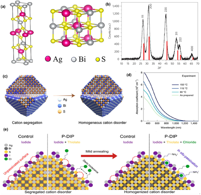
 DownLoad:
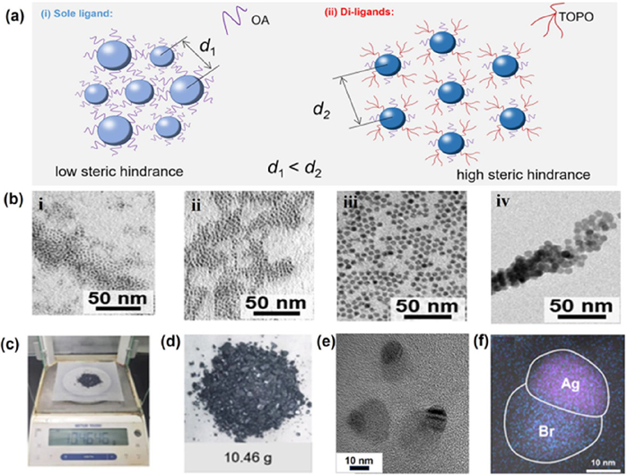
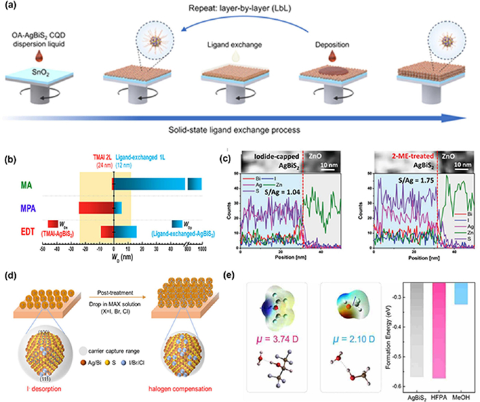
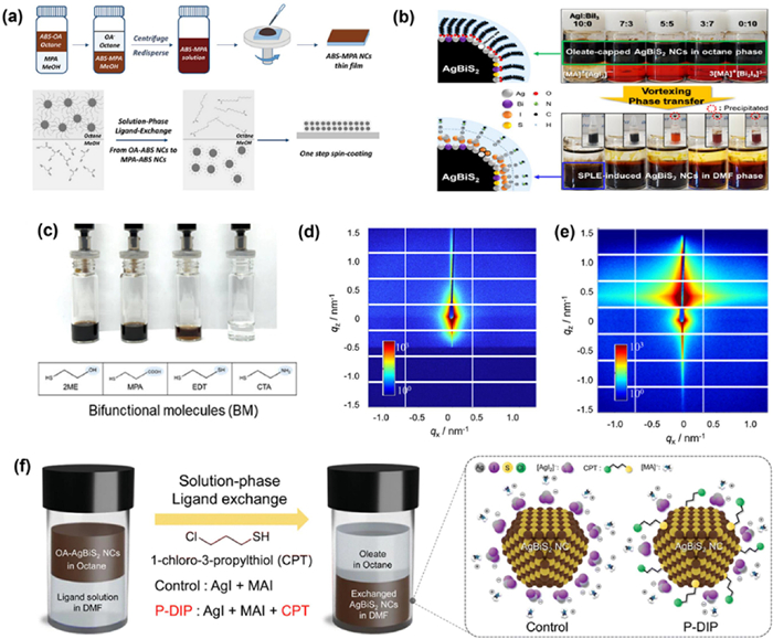
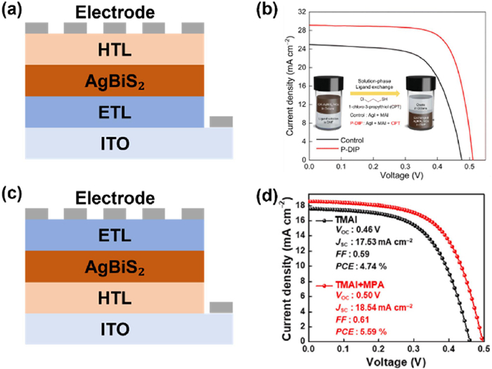
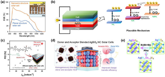
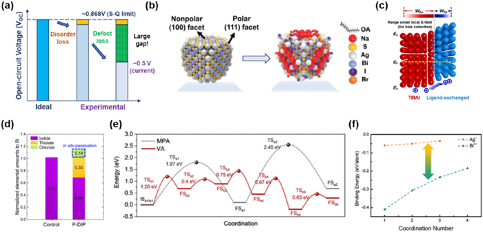
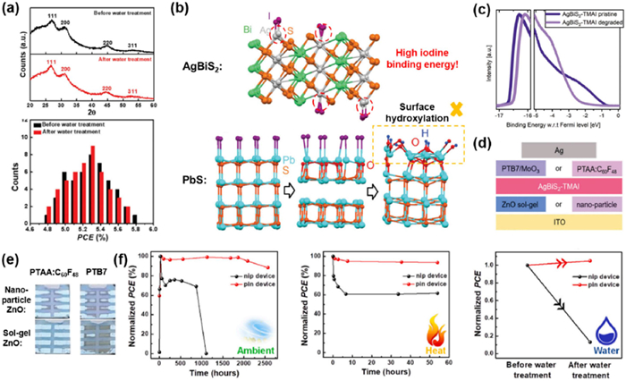

 下载:
下载:


