State Key Laboratory of Chemo and Biosensing, College of Chemistry and Chemical Engineering, Hunan University, Changsha 410082, China
b.
Key Laboratory of Food & Environment & Drug Monitoring and Testing of Universities in Hunan Province, Hunan Police Academy, Changsha 410138, China
* Corresponding author. E-mail address: liusong@hnu.edu.cn (S. Liu). 1 These authors contributed equally to this work.
Received Date:
19 June 2025 Accepted Date:
28 September 2025 Revised Date:
25 September 2025 Available Online:
15 February 2026
Abstract:
The hydrogen evolution reaction (HER) is crucial for hydrogen production and sustainable energy storage. Molybdenum disulfide (MoS2), a representative transition metal dichalcogenides (TMDs), shows potential as an HER catalyst but suffers from limited performance due to poor charge transfer and interfacial effects. Here, we report a salt-assisted chemical vapor deposition (CVD) method for synthesizing high-quality tungsten ditelluride (WTe2) with tunable morphologies using alkali halides (NaCl, KCl and LiCl). The prepared WTe2 nanoribbons and hexagonal nanosheets exhibit morphology-dependent electrical conductivity, with nanosheets showing superior performance. To evaluate WTe2 as a contact electrode, WTe2−MoS2 heterostructures were fabricated and compared with graphene-MoS2 counterparts. The WTe2−MoS2 heterostructure exhibits a superior Tafel slope of 111.57 mV/dec and an overpotential of 298 mV at -10 mA/cm2, significantly outperforming graphene-based electrodes. This improvement is attributed to the excellent conductivity of WTe2 and reduced interfacial Schottky barriers. Moreover, we systematically investigate the influence of WTe2 thickness on HER performance and assess the electrochemical durability and structural stability of the heterostructure, further confirming the effectiveness of WTe2 as a contact electrode for enhancing the HER activity of MoS2. This study offers a novel approach for enhancing the HER performance of MoS2 through controlled WTe2 growth and application as a contact electrode. Our findings provide valuable insights into the synthesis of high-quality WTe2 and broaden the potential applications of two-dimensional materials in energy catalysis.
The hydrogen evolution reaction (HER) is a key step in water splitting for hydrogen production and plays a crucial role in renewable energy storage and the development of the hydrogen economy [1-4]. With the increasing global demand for clean energy, the development of efficient, stable and low-cost electrocatalysts has become a major research focus [5-7]. Transition metal dichalcogenides (TMDs) have attracted significant attention in HER research due to their unique electronic structures and excellent catalytic activities [8-10]. Among them, molybdenum disulfide (MoS2) exhibits platinum-like catalytic characteristics owing to its near-zero Gibbs free energy change (ΔGH*) [11]. Experimental studies have shown that MoS2 demonstrates high activity in HER [12,13], however, its catalytic efficiency is still limited by factors such as charge injection efficiency [14,15], interfacial effects [16], and the material's microstructure [17]. Therefore, enhancing the HER catalytic performance of MoS2 remains a key research challenge.
Optimizing charge injection into MoS2 is an effective strategy to improve its catalytic performance. Due to its relatively large bandgap and limited intrinsic conductivity, the catalytic efficiency of MoS2 is restricted by electron transport. Choosing an appropriate contact electrode to reduce interfacial Schottky barriers and enhance charge carrier mobility is a feasible approach [18-21]. In recent years, tungsten ditelluride (WTe2) has emerged as a promising contact electrode for improving the HER performance of MoS2 [22]. WTe2 exhibits high electrical conductivity [23], excellent interfacial contact properties, and strong spin-orbit coupling effects [24], which facilitates efficient electron injection from an external circuit into MoS2, thereby enhancing catalytic efficiency. However, the controlled synthesis of WTe2 remains challenging due to the low chemical reactivity of tellurium (Te) with tungsten (W) sources, which makes it difficult to grow WTe2. Besides, the low phase stability of WTe2 at high temperatures can lead to phase transitions or structural defects, which could degrade its performance as a contact electrode.
To address these challenges, chemical vapor deposition (CVD) has been identified as a promising solution [25]. CVD can realize precise growth control and scalability, which enables effective control over the thickness, morphology and structural stability of WTe2 [26-30]. Based on this, we report a salt-assisted CVD method for synthesizing high-quality WTe2. By employing different alkali metal halide salts, we achieved morphology control of WTe2, obtaining nanoribbons and hexagonal nanosheets. By investigating the effects of growth time and salt dosage, we map out the complete morphology evolution process. Based on the fundamental principles of salt-assisted growth, intermediate metal oxyhalides follow a vapor-solid-solid (VSS) growth mechanism, whereas molten salts derived from metal oxides follow a vapor-liquid-solid (VLS) pathway. Building on these insights, we propose a corresponding growth mechanism to clarify the distinct roles of various alkali metal salts in governing the morphological evolution of WTe2. Additionally, we examine the stability of WTe2 with different morphologies in air and observe that thinner samples are more prone to oxidation and degradation, suggesting that vacuum storage is a more effective preservation method. Subsequently, we evaluate the electrical properties of the synthesized WTe2 samples and find that the nanosheets exhibit higher conductivity than the nanoribbons. Based on the excellent electrical conductivity and interfacial contact properties of WTe2, we further construct the WTe2−MoS2 and graphene-MoS2 heterostructures to investigate the effect of WTe2 as a contact electrode on the catalytic behavior of MoS2. Experimental results show that the WTe2−MoS2 heterostructure exhibits a Tafel slope of 111.57 mV/dec and an overpotential of 298 mV at −10 mA/cm2, which is significantly better than that of graphene as a contact electrode. Meanwhile, we systematically investigate the effect of WTe2 thickness on HER performance and evaluate the electrochemical durability and structural stability of the device, further validating the effectiveness of WTe2 as a contact electrode for enhancing the HER activity of MoS2. This study not only presents a novel strategy for enhancing the HER catalytic performance of MoS2 but also provides an experimental basis for the controlled growth of high-quality WTe2, laying the groundwork for the broader application of two-dimensional (2D) materials in energy catalysis.
To prepare atomically thin WTe2, a salt-assisted CVD method was employed, as illustrated in Fig. 1a. With sodium chloride (NaCl) salt, WTe2 exhibits nanoribbon morphology, whereas, with potassium chloride (KCl) salt, the WTe2 morph into hexagonal nanosheets or dendrites. The addition of alkali metal halide salt (e.g., NaCl or KCl) can significantly lower the melting point of metal oxides, thereby enhancing the precursor concentration for WTe2 growth. This strategy has been widely used in the synthesis of other two-dimensional TMDs such as MoS2 [31] and WS2 [32]. Notably, the type of salt plays a critical role in controlling the morphology of WTe2 and this mechanism will be discussed in detail later. Optical microscopy images (OM) of WTe2 samples are presented in Figs. 1b and c, clearly showing two distinct morphologies: Nanoribbons and hexagonal nanosheets. To evaluate the thickness of the CVD-grown 2D WTe2, atomic force microscopy (AFM) characterization was performed (Figs. 1d and e). The thickness of the WTe2 nanoribbon is measured to be approximately 4.75 nm, while the hexagonal nanosheet has a thickness of 3.43 nm. Besides, we have also measured the thickness of other nanoribbons and hexagonal nanosheets in SiO2/Si substrate, which are available in Fig. S1 (Supporting information). Their thicknesses are all < 10 nm. To confirm the composition and crystal structure of the obtained samples, Raman spectroscopy was conducted as shown in Fig. 1f. Seven typical Raman peaks are observed in both the nanoribbon and hexagonal nanosheet samples, located at 82.4, 88.7, 108.8, 115.9, 131.5, 161.3 and 209.0 cm-1, which correspond to the A12, B110, A24, A23, A41, A17 and A19 modes of 1T'-WTe2, respectively [22]. These Raman peaks can be categorized into two types: interlayer and intralayer vibration modes. Specifically, 88.7, 108.8, 115.9 and 131.5 cm-1 are associated with intralayer vibrations, while 82.4, 161.3 and 209.0 cm-1 correspond to interlayer vibrations. The corresponding top and side views of the atomic structure of 1T'-WTe2 are presented in Fig. 1g. To further verify the spatial uniformity of the WTe2 samples, Raman mappings were performed (Figs. 1h and i). Our results demonstrate that the WTe2 samples exhibit excellent spatial homogeneity with no detectable impurities.
Figure 1
Figure 1.
Synthesis and characterizations of CVD-grown WTe2. (a) Schematic diagram of the CVD growth process. (b, c) OM images of as-grown WTe2 nanoribbon and hexagonal WTe2, respectively. (d, e) AFM images of as-grown WTe2 nanoribbon and hexagonal WTe2, respectively. Inset: corresponding height profile analyses. (f) Raman spectra of as-grown WTe2. (g) Top and side views of the crystal structure of 1T'-WTe2. (h, i) Raman intensity mappings of WTe2 nanoribbon and hexagonal WTe2, respectively.
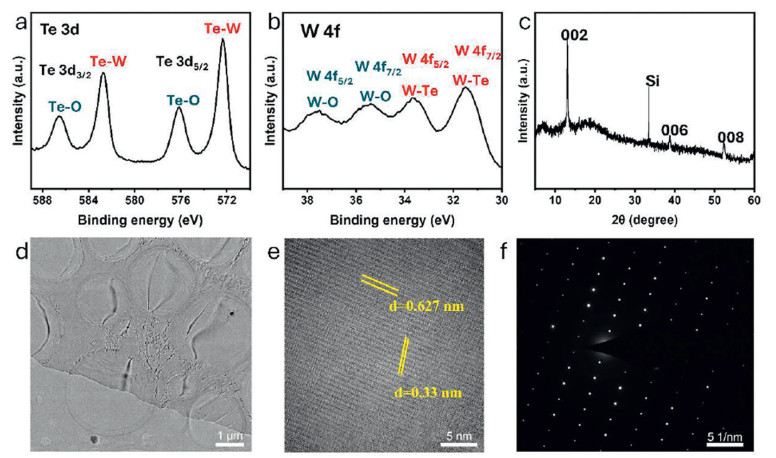
The chemical states and elemental compositions of obtained samples were characterized by X-ray photoelectron spectroscopy (XPS), with the results being shown in Figs. 2a and b. The Te 3d spectrum can be well-fitted by two peaks located at 583.7 eV (Te 3d3/2) and 573.3 eV (Te 3d5/2), which are associated with W-Te bonds. This confirms the successful formation of WTe2 and demonstrates that CVD process effectively overcomes the low chemical reactivity of Te. Additionally, two oxidation peaks (binding energies at 585.4 and 575.1 eV) are clearly observed in the Te 3d spectrum, attributed to Te-O bonding. These indicate the presence of a small amount of oxidized Te in the material, which may be related to the inherent instability of WTe2. The binding energies at ≈33.7 eV and ≈31.5 eV are attributed to W 4f5/2 and W 4f7/2, respectively, confirming the presence of W-Te bonds. Meanwhile, the other two peaks are attributed to W-O bonds. In addition, the X-ray diffraction (XRD) result of corresponding samples deposited on the SiO2/Si substrate confirms the formation of WTe2 (Fig. 2c). The main diffraction peaks in the XRD spectrum are consistent with those of orthorhombic WTe2, with peaks at 13.00°, 38.79° and 52.35° corresponding to the (002), (006) and (008) crystal planes, respectively. Notably, the diffraction peak at 13.00° exhibits the strongest intensity, indicating that the WTe2 surface is parallel to the SiO2/Si substrate. Therefore, WTe2 with good crystalline orientation can be achieved through salt-assisted atmospheric-pressure CVD. To understand the crystalline structure and quality of CVD-derived atomically thin WTe2, the transferred samples were characterized by transmission electron microscopy (TEM). The low-magnification TEM images of the WTe2 nanosheet are shown in Fig. 2d. The well-defined morphologies and highly transparent properties indicate the perfect crystalline qualities and ultrathin features. Fig. 2e clearly exhibits lattice fringes with spacings of 0.627 and 0.33 nm, which are attributed to the (010) and (101) crystal planes, respectively. The selected area electron diffraction (SAED) can effectively reflect the crystal quality over a large area. As shown in Fig. 2f, the diffraction spots present regular shape, like orthogonal atomic lattice. This result is highly consistent with the structural characteristics of the orthorhombic WTe2, thus confirming that WTe2 has good crystallinity.
Figure 2
Figure 2.
Chemical states and atomic structure of CVD-grown WTe2. (a, b) XPS spectrum of as-grown WTe2. (c) XRD pattern of as-grown WTe2. (d) Low-magnification TEM image of transferred WTe2 nanosheet. (e) Atomic-resolution TEM image of transferred WTe2 nanosheet. (f) Corresponding SAED pattern of WTe2.
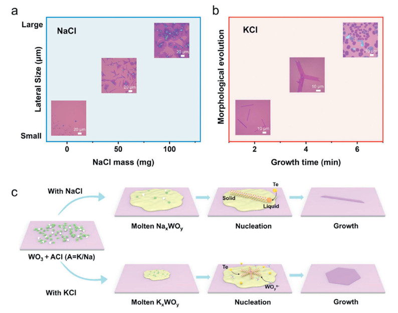
To investigate the growth mode of WTe2 in-depth, we systematically adjusted the growth conditions, focusing on the effects of alkali metal halide types and their quantities, growth time and the introduction of H2 on the morphology of WTe2. Experimental results indicate that the type of salt and the growth time significantly influence the morphology of WTe2. Figs. 3a and b illustrate the changes in the size and morphology of WTe2 with varying NaCl amounts and the effect of growth time when using KCl as a flux agent. Fig. 3a shows that without NaCl, the product on the silicon substrate appeared as granules, with no deposition of 2D material. When 50 mg of NaCl was added as flux agent, WTe2 nanoribbons with lengths up to 100 µm were obtained. As the NaCl concentration increased, WTe2 gradually exhibited a thin-film growth trend. When the NaCl concentration reached 100 mg, a large-area polycrystalline film formed on the substrate. However, the film exhibited cracks and grain boundaries, resulting in relatively low quality. With a fixed NaCl concentration, extending the growth time leaded to the gradual thickening of WTe2 nanoribbons while maintaining their morphology (Fig. S2 in Supporting information). Previous studies have shown that the key to WTe2 growth is the controlled introduction of hydrogen gas (H2) during the reaction process. In this study, we also investigated the effect of H2 reaction time on the growth process by controlling this single variable (Fig. S3 in Supporting information). The results show that continuous introduction of H2 produced elongated WTe2 nanoribbons, with lengths reaching 50 µm and widths below 3 µm. When H2 was introduced briefly during the reaction and then turned off at the end, 2D WTe2 structures were formed, however, etching effects were observed. These results indicate that H2 reaction time directly affects material morphology, playing a dual role in both promoting growth and inducing etching in the CVD process of WTe2. When KCl was used as a flux agent, the morphology of WTe2 evolved from nanoribbons to dendritic structures and eventually to hexagonal nanosheets as the growth time increased (Fig. 3b). Fig. S4 (Supporting information) displays thin-layer samples with several branches. The six-branched WTe2 exhibits high symmetry, with each branch forming a 60° angle with its neighbors. In the five-branched WTe2, one angles is 120°, while the remaining angles are all 60°. Subsequently, we further confirmed the composition of dendritic WTe2 using Raman spectroscopy. The specific Raman peaks of Fig. S5a (Supporting information) are consistent with that of 1T'-WTe2 in Fig. 1f. Raman mappings of five and six-branched WTe2, with peak fitting at ~162 cm-1 and ~211 cm-1, reveals distinct characteristics. The intensity of the A17 peak gradually increases from the center toward the branch edges, while the intensity of the A19 characteristic peak varies in different directions (Figs. S5b-e in Supporting information). The corresponding AFM and scanning electron microscope (SEM) characterization results of six-branched WTe2 are shown in Fig. S6 (Supporting information). The sample thickness increased gradually from the edges toward the center, with a maximum thickness of 32.08 nm and an edge thickness of only 11.87 nm. Based on these observations above, we assume that salts play a crucial role in the assisted growth of WTe2.
Figure 3
Figure 3.
Growth mechanism of CVD-grown WTe2. (a) Influence of NaCl mass on the WTe2 morphology. (b) Influence of growth time (with KCl) on the WTe2 morphology (c) Schematic diagram of growth mechanism about alkali metal halide types leading to different WTe2 morphologies.
Alkali metals (Li, Na, K) are essential components of alkali metal halide salts. Although NaCl and KCl differ only in their alkali metal components, they lead to distinctly different morphologies in the obtained WTe2 samples. Herein, we propose the possible growth mechanism as shown in Fig. 3c. Firstly, alkali metal halide salts react with tungsten oxide powder to form two types of intermediates, WOxCly and AxWOy (A = K or Na) [33,34]. These intermediates significantly reduce the melting point of WO3, thereby facilitating its reaction with Te powder. The WOxCly intermediate, formed by the reaction of halogens with metal oxides, is a metal oxyhalide compound that reacted with Te via VSS mode [31,35,36]. Since KCl and NaCl share the same halide ions, their roles in the VSS mechanism should be identical. NaxWOy and KxWOy are tungstates formed by the reaction of alkali metals with metal oxides and their reaction with Te powder follows VLS mode [31,35,36]. However, Na2WO4 has a significantly lower melting point than K2WO4 and exhibits greater solubility [37]. Consequently, in the VLS mode, NaxWOy has higher epitaxial mobility than KxWOy, making it less likely to accumulate on the substrate and more inclined to form WTe2 nanoribbon upon reacting with Te. In contrast, KxWOy has a lower epitaxial mobility and a smaller molten mass than NaxWOy. As a result, KxWOy needs to accumulate to a certain concentration on the substrate before gradually diffusing outward, ultimately forming dendritic WTe2 structures, which further evolve into hexagonal nanosheets. Notably, we find that this salt-assisted CVD method exhibits excellent universality, enabling the fabrication of nanoribbon-like, dendritic and hexagonal WTe2 samples on different substrates such as sapphire and mica (Figs. S7 and S8 in Supporting information). This lays a solid foundation for further exploration of controlled morphology growth and the applications of WTe2. To further validate the influence of alkali metal halide type on WTe2 morphology, we introduced lithium chloride (LiCl) as an additional salt under the same growth conditions. As shown in Fig. S9 (Supporting information), the resulting WTe2 structures remain as elongated nanoribbons, consistent with those synthesized using NaCl. Optical and AFM characterizations reveal narrow, flat nanoribbons with uniform thickness and Raman spectra confirms the formation of good crystalline WTe2. The preserved WTe2 nanoribbon morphology supports our proposed VSL growth mechanism. Compared with KCl, LiCl exhibits higher solubility and forms an intermediate (Li2WO4) with a lower melting point (742 ℃), which is close to that of Na2WO4 (698 ℃) but significantly lower than K2WO4 (921 ℃). This favors the generation of volatile intermediates necessary for ribbon-like growth. The consistent morphological trends observed across Li+, Na+, K+ salts highlight the critical role of alkali halide selection in controlling the structural evolution of WTe2.
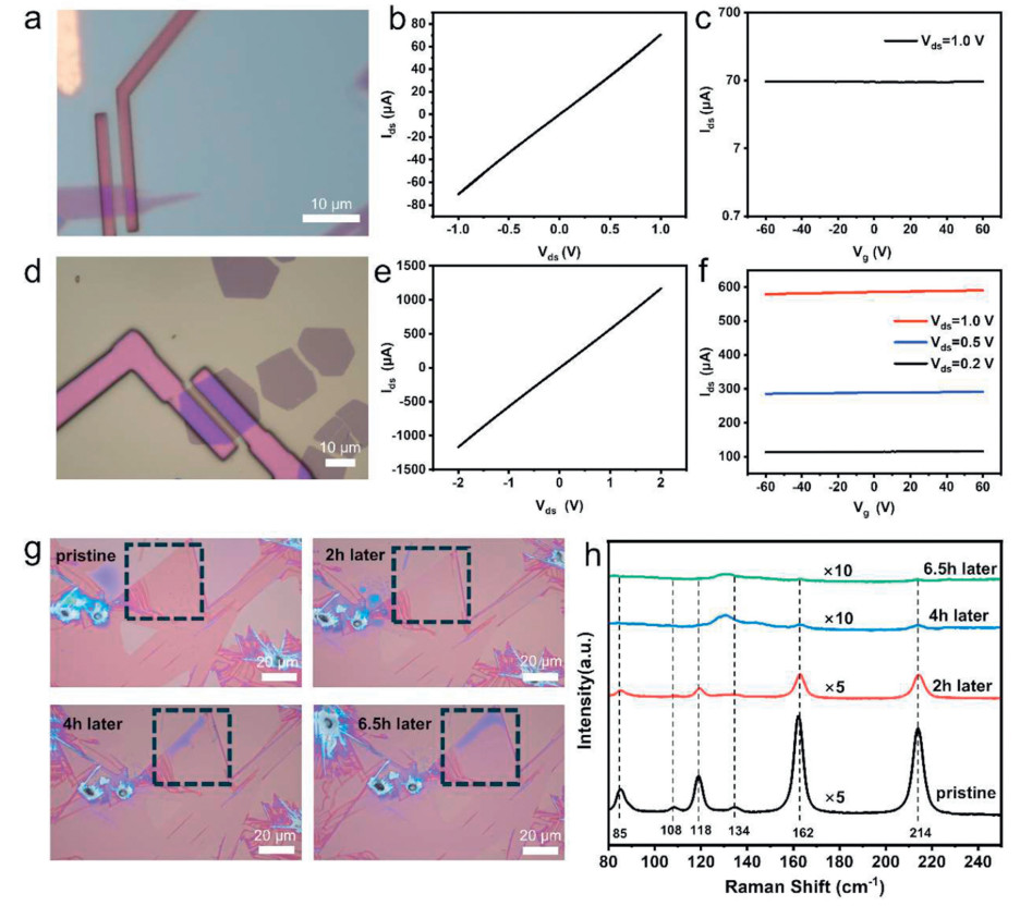
To investigate the electrical properties of the synthesized WTe2 samples, two-terminal WTe2 devices were fabricated on a SiO2/Si substrate. The Si substrate can modulate the electrostatic potential of the WTe2 device, similar to a field-effect transistor (Figs. 4a and d). The output characteristics of the WTe2 nanoribbon exhibit a linear and symmetric relationship, indicating the formation of good ohmic contacts. When the source-drain voltage (Vds) was applied to 0.35 V, the source-drain current (Ids) was 35 µA while when Vds = 1.0 V, Ids increased to 70 µA, demonstrating the good conductivity of WTe2 nanoribbon (Fig. 4b). In the transfer curve (Fig. 4c), regardless of the gate voltage variation (from −60 V to 60 V), the current remained constant at 70 µA. This indicates that the gate voltage has no significant effect on the source-drain current, suggesting the metallic behavior of WTe2 nanoribbons. As for the hexagonal WTe2 nanosheet, the electrical results exhibit its metallic properties and demonstrate a higher current than the WTe2 nanoribbon. The output curve shows that with a constant gate voltage, the Ids exhibits a linear relationship with the Vds (Fig. 4e). This indicates that the transistor operated in the linear region, where its output current can be controlled by the input voltage and the current variation was predictable. The output curve passed through the origin (0, 0), indicating that the transistor's leakage current can be ignored. This suggests that in the absence of an applied voltage, there is no leakage current, demonstrating good turn-off characteristics. Fig. 4f presents the transfer curve of hexagonal WTe2 nanosheet, under Vds = 1.0 V, Vds = 0.5 V, and Vds = 0.2 V, the Ids remained unchanged regardless of the gate voltage, forming a straight line with negligible hysteresis.
Figure 4
Figure 4.
Electrical properties of WTe2 devices and their air stability. (a) OM image of the WTe2 nanoribbon device and (b) its corresponding output and (c) transfer characteristic curves. (d) OM image of the hexagonal WTe2 nanosheet device and (e) its corresponding output and (f) transfer characteristic curves. (g) OM images of as-grown WTe2 sample after exposure to air for different time periods. (h) Corresponding Raman spectra of as-grown WTe2 sample after exposure to air for different time periods.
Although WTe2 exhibits excellent electrical conductivity, thin-layer WTe2 is highly sensitive to the environment and has poor stability, with oxidation-induced decomposition significantly reducing its conductivity. We conducted relevant studies on this issue. Figs. 4g and h present the changes in optical images and Raman spectra of WTe2 thin films in the same region after different durations of air exposure. The as-grown WTe2 exhibits six characteristic peaks in the Raman spectrum (85, 108, 118, 134, 162 and 214 cm-1). After 2 h of air exposure, the intensity of the 162 and 214 cm-1 peaks decreased significantly. After 6.5 h, these two primary peaks almost completely disappeared. This phenomenon is consistent with the two distinct Te-O oxidation peaks observed in the XPS spectra of the Te 3d, further confirming the instability of WTe2. WTe2 with different morphologies underwent varying degrees of decomposition after air exposure for several minutes to several days. Light pink nanosheets rapidly decomposed within 2 min, with their sharp edges becoming blurred, after which the color stabilizes. WTe2 nanoribbons exhibited noticeable damage and material loss under an optical microscope after several days of air exposure (Fig. S10 in Supporting information). Hexagonal nanosheets, when stored in a vacuum-sealed environment within a vacuum drying chamber for 57 days, retained the same morphology as when they were first grown with clear boundaries, no significant color change, and no visible signs of oxidation (Fig. S11 in Supporting information). This indicates that vacuum storage significantly reduces the oxidation rate of the samples, which is beneficial for device fabrication and the study of the intrinsic properties of the material.
Based on the unique metallic properties of WTe2 and its excellent electrical transport capability, we selected WTe2 as the electrode material to replace the traditional gold electrode, aiming to construct on-chip electrochemical devices and optimize HER catalytic performance of MoS2. Meanwhile, graphene was introduced as a comparative electrode to compare the influence of two different electrode materials on the HER performance of MoS2. Due to the poor adhesion of gold on the SiO2/Si substrate, a 5 nm thick Cr wetting layer was introduced in the experiment to construct a microreactor and ensure stable electrical contact with MoS2. During the experiment, only the basal plane of MoS2 was exposed to the electrolyte for HER performance characterization. The configurations of heterostructures are illustrated in the schematic diagram (Fig. 5a) and the optical image (Figs. 5b and c). The on-chip electrochemical device construction process of specific WTe2−MoS2 heterostructure is shown in Fig. S12 (Supporting information).
Figure 5
Figure 5.
The effect of WTe2 as electrode material on HER activity of MoS2 (a) Cross-sectional schematic view of configurations of heterostructures. (b) OM image of graphene-MoS2 heterostructure with MoS2 basal plane exposed. (c) OM image of WTe2−MoS2 heterostructure with MoS2 basal plane exposed. (d) Polarization curves of graphene-MoS2 and WTe2−MoS2 heterostructures for the HER in 0.5 mol/L H2SO4. (e) Their corresponding Tafel plots of (d).
The experimental results further verify the superior performance of the WTe2 electrode. Figs. 5d and e present the polarization curves and corresponding Tafel slopes of the WTe2−MoS2 and graphene-MoS2 heterostructures. At the current density of −10 mA/cm2, the overpotential of the WTe2−MoS2 heterostructure is 298 mV with a Tafel slope of 111.57 mV/dec, whereas the graphene-MoS2 heterostructure exhibits a significantly higher overpotential of 491 mV and a Tafel slope of 157.5 mV/dec. This result indicates that WTe2, as a contact electrode, can significantly enhance the HER catalytic activity of MoS2, outperforming graphene electrodes.
This performance enhancement can be attributed to the excellent electrical conductivity of WTe2 and its effective improvement of electron injection and transport in MoS2. Additionally, the theoretical work functions of monolayer MoS2 and WTe2 are 4.36 and 4.5 eV, respectively, with relatively close Fermi levels [23,38,39]. To experimentally determine the energy level alignment within the WTe2−MoS2 heterostructure, we performed kelvin probe force microscopy (KPFM) measurements on both materials under our specific growth conditions. As shown in Fig. S13 (Supporting information), WTe2 and MoS2 exhibit measured surface potentials of 223 mV and 131 mV, respectively, while the standard gold reference (Au) shows −105 mV. The work functions of WTe2 and MoS2 were calculated using the following equation:
$
e V_{\text {cpd }}=\phi_{\text {tip }}-\phi_{\text {sample }}
$
(1)
In which, Vcpd represents contact potential difference (CPD) between the measurement probe and the sample, ɸtip represents the work function of the probe, and ɸsample represents the work function of the sample. Given that the work function of Au is 5.1 eV, the work functions of WTe2 and MoS2 were estimated to be 4.77 and 4.86 eV, respectively. This relatively small difference results in near Fermi level alignment and a low Schottky barrier at the heterointerface, facilitating interfacial electron transport, improving electron transfer efficiency and consequently enhancing the electrocatalytic activity of MoS2. The experimental results suggest that charge injection efficiency plays a crucial role in enhancing catalytic activity. Through this strategy, the inherently low catalytic activity of the TMDs basal plane is activated, providing a new research direction for further optimizing HER performance.
To further investigate the effect of contact electrode thickness on the electrocatalytic performance of WTe2−MoS2 heterostructures, we fabricated a series of devices using WTe2 nanoribbons with controlled thicknesses of 5.8, 12.2, 27.2, 38.6 and 56.6 nm, while keeping the exposed MoS2 geometric configuration consistent. The optical microscope images and corresponding AFM height profiles of the devices are shown in Fig. S14 (Supporting information), confirming the uniformity in lateral dimensions and the variation in vertical thickness of WTe2 contacts.
HER polarization curves and Tafel plots (Fig. S15 in Supporting information) reveal a consistent enhancement in catalytic activity with increasing WTe2 thickness. Specifically, both the overpotential at −100 mA/cm2 and the Tafel slope decrease monotonically as the WTe2 thickness increases, suggesting more favorable charge transfer kinetics. Since only MoS2 is in direct contact with the electrolyte, the observed performance improvement is attributed to the interfacial properties modulated by WTe2 thickness. Thicker WTe2 layers provide enhanced structural integrity, reduced surface roughness and improved interface conformity during the dry transfer process. These factors contribute to a cleaner van der Waals interface and more efficient charge injection from the WTe2 electrode into the MoS2 basal plane. In contrast, ultrathin WTe2 flakes (e.g., 5.8 nm) are more susceptible to oxidation or transfer-induced defects, which may introduce interfacial barriers or disrupt the electronic coupling.
No performance degradation or saturation is observed within the studied thickness range, indicating that WTe2 thickness is a key parameter for optimizing interfacial charge transport in the heterostructure. These results emphasize the importance of contact engineering in on-chip electrochemical devices, particularly when employing 2D metallic contacts such as WTe2.
To evaluate the electrochemical and structural stability of the WTe2−MoS2 heterostructure, 500 cycles cyclic voltammetry (CV) test was conducted in 0.5 mol/L H2SO4 within the potential range of 0.2~−0.25 V vs. RHE on the on-chip electrochemical device. As shown in Fig. S16 (Supporting information), the device maintains relatively stable HER performance throughout the cycling process, with only a slight decrease in current density, indicating good durability under repetitive operation. In addition, optical characterizations were conducted before and after HER testing. As shown in Figs. S17a and b (Supporting information), the optical images of the same device reveal that the top MoS2 layer undergoes partial degradation after cycling, while the underlying WTe2 remains intact and morphologically stable. Raman spectra acquired at the marked positions (blue: before HER; orange: after HER) show that the characteristic MoS2 peaks (A1g and E2g1) decrease significantly in intensity after HER, whereas WTe2-related peaks remain well preserved (Fig. S17c in Supporting information). These results confirm the robust electrochemical performance and structural resilience of the WTe2−MoS2 heterostructure, highlighting WTe2 as a stable contact layer during HER operation.
In this study, we have successfully developed a salt-assisted CVD method for synthesizing high-quality WTe2 with controlled morphologies. By utilizing different alkali metal halide salts (NaCl, KCl and LiCl), we achieve precise morphology control, producing both nanoribbons and hexagonal nanosheets. Systematic investigations into growth time, salt dosage, and salt types reveal the underlying growth mechanisms and demonstrate the versatility of this approach. Electrical measurements confirm that hexagonal nanosheets exhibit higher conductivity than nanoribbons. Furthermore, we constructed WTe2−MoS2 heterostructures and demonstrated their superior HER performance compared to graphene-based electrodes. The WTe2−MoS2 heterostructure achieves a Tafel slope of 111.57 mV/dec and an overpotential of 298 mV at −10 mA/cm2 outperforming graphene electrodes due to the excellent conductivity of WTe2 and improved electron injection and transport in MoS2. Besides, we further evaluated the HER-related performance of our system by investigating the effect of WTe2 thickness and conducting durability and structural stability tests, confirming improved interfacial charge transport and acceptable long-term stability of the WTe2−MoS2 heterostructure. This study provides a novel approach for enhancing HER performance through the controlled growth of WTe2 and its application as a contact electrode. Our findings offer valuable insights into the synthesis of high-quality WTe2 and expand the potential applications of two-dimensional materials in energy catalysis, paving the way for further advancements in hydrogen production technologies.
Declaration of competing interest
The authors declare that they have no known competing financial interests or personal relationships that could have appeared to influence the work reported in this paper.
H.R. Rasouli, N. Mehmood, O. Çakıroğlu, T.S. Kasırga, Nanoscale 11 (2019) 7317–7323. doi: 10.1039/c9nr00614a
[37]
D. Li, S. Yoshida, B. Siritanaratkul, et al., ACS Catal. 11 (2021) 14237–14248. doi: 10.1021/acscatal.1c04206
[38]
J.M. Woods, J. Shen, P. Kumaravadivel, et al., ACS Appl. Mater. Interfaces 9 (2017) 23175–23180. doi: 10.1021/acsami.7b04934
[39]
S.Y. Lee, U.J. Kim, J. Chung, et al., ACS Nano 10 (2016) 6100–6107. doi: 10.1021/acsnano.6b01742
Figure 1
Synthesis and characterizations of CVD-grown WTe2. (a) Schematic diagram of the CVD growth process. (b, c) OM images of as-grown WTe2 nanoribbon and hexagonal WTe2, respectively. (d, e) AFM images of as-grown WTe2 nanoribbon and hexagonal WTe2, respectively. Inset: corresponding height profile analyses. (f) Raman spectra of as-grown WTe2. (g) Top and side views of the crystal structure of 1T'-WTe2. (h, i) Raman intensity mappings of WTe2 nanoribbon and hexagonal WTe2, respectively.
Figure 2
Chemical states and atomic structure of CVD-grown WTe2. (a, b) XPS spectrum of as-grown WTe2. (c) XRD pattern of as-grown WTe2. (d) Low-magnification TEM image of transferred WTe2 nanosheet. (e) Atomic-resolution TEM image of transferred WTe2 nanosheet. (f) Corresponding SAED pattern of WTe2.
Figure 3
Growth mechanism of CVD-grown WTe2. (a) Influence of NaCl mass on the WTe2 morphology. (b) Influence of growth time (with KCl) on the WTe2 morphology (c) Schematic diagram of growth mechanism about alkali metal halide types leading to different WTe2 morphologies.
Figure 4
Electrical properties of WTe2 devices and their air stability. (a) OM image of the WTe2 nanoribbon device and (b) its corresponding output and (c) transfer characteristic curves. (d) OM image of the hexagonal WTe2 nanosheet device and (e) its corresponding output and (f) transfer characteristic curves. (g) OM images of as-grown WTe2 sample after exposure to air for different time periods. (h) Corresponding Raman spectra of as-grown WTe2 sample after exposure to air for different time periods.
Figure 5
The effect of WTe2 as electrode material on HER activity of MoS2 (a) Cross-sectional schematic view of configurations of heterostructures. (b) OM image of graphene-MoS2 heterostructure with MoS2 basal plane exposed. (c) OM image of WTe2−MoS2 heterostructure with MoS2 basal plane exposed. (d) Polarization curves of graphene-MoS2 and WTe2−MoS2 heterostructures for the HER in 0.5 mol/L H2SO4. (e) Their corresponding Tafel plots of (d).


 DownLoad:


 下载:
下载:


