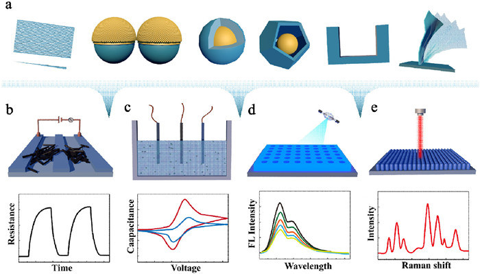
Figure 1.
(a) Micro- and nano-structures. (b) Chemiresistive sensing. (c) Electrochemical sensing. (d) Fluorescence sensing. (e) SERS sensing.
Pushing the frontiers: Chip-based detection based on micro- and nano-structures
Meihui Liu , Xinyuan Zhou , Xiao Li , Zhenjie Xue , Tie Wang

Early diagnosis of diseases is closely related to people's life and health, but the current main way of disease diagnosis requires people to go to the hospital for examination, which will lead to the disease not being discovered in time and delaying the best treatment time. Therefore, it is crucial to develop a disease diagnosis method that can be detected online in real time. Sensors have the advantages of high sensitivity, rapid and real-time response, ease of operation, and portability [1–3], which have become essential tools in medical screening campaigns [4–6]. They possess the ability to effortlessly convert physical, chemical, biological, and various other signals acquired into readily recognizable forms such as electrical or optical signals. NPs possess an aptness in the sensing operations due to they exhibit distinctive behaviors owing to the minute dimensions, expanded surface area, boundaries, and quantum effects. However, the design and construction of NPs-based assemblies, with a focus on their size, shape, and morphology, has arisen as a developing area of interest due to the limitations of conventional NPs in meeting specific application requirements [7]. The primary grounds for this assertion relate to the fact that the sensitivity decreases due to the heterogeneous reaction at the liquid-solid interface in future chip-based detection. As a consequence, it is essential to systematically investigate interparticle interactions and structure-property correlations. Both the bottom-up and top-down approaches are employed for the manufacture of NP assemblies. The utilization of sophisticated fabrication techniques facilitates the modification of the microstructure and morphology of assemblies, and their various morphologies and structures impart special properties to the materials [8]. These techniques have introduced an abundance of variations in the micro- and nano-structure dimensionality, which have been employed to enhance the properties of sensors, including response speed, sensitivity, selectivity, stability, and detection range [9–13].
The formation of micro- and nano-structures through the arrangement of NP assemblies can be induced by molecular interactions, such as van der Waals interactions, electrostatic interactions, depletion interactions, and dipole-dipole interactions. The modification of interparticle interactions is also achieved by altering solvent type, reaction temperature, interface conditions associated with colloidal solution, and vapor pressure [14]. The synthesis of micro- and nano-structures with shape-controlled one-dimensional (1D), thickness-controlled two-dimensional (2D), and morphology-controlled three-dimensional (3D) structures has been accomplished [15,16]. Furthermore, considerable effort has been dedicated to fine-tuning and augmenting the physicochemical characteristics of varying categories of micro- and nano-structures, and some researchers have noted the highly intriguing dynamic properties that these micro- and nano-structures possess [17,18]. These deformable structures engage in active alteration of their initial state in response to environmental changes via procedures such as deformation/motion, self-replication, perception, self-regulation, and self-repair-while taking in and releasing energy.
The importance of micro- and nano-structures is becoming more apparent. Several previous reviews have introduced micro- and nano-structures for sensing based on different key points with specialized focus, such as different morphological metal-organic framework (MOF) micro- and nano-structures [19], core-shell structured molecularly imprinted materials [20], hollow micro- and nano-structured ceria-based materials [8], and solid-state nanopore sensors [1]. For the low efficiency of interface heterogeneous reaction, it is possible to improve the performance of the sensor in terms of sensitivity and detection limit by designing the interface micro- and nano-structures reasonably. In recent years, there have been more and more reports on the interfacial micro- and nano-structures modulated sensing methods, making it a highly competitive research field. Unfortunately, there is a lack of reviews to summarize this exciting and rapidly growing field. Herein, we begin by providing an overview of the sensing mechanisms and prevalent difficulties about four sensors including chemiresistors, electrochemical sensors, fluorescence sensors, and SERS sensors, which are widely used in life and health monitoring. We then discuss recent advancements in various types of micro- and nano-structures used in sensors, categorized as wire, layered, core-shell, hollow, concave, and deformable structures, according to structural characteristics (Fig. 1). These structures change the size, shape, and morphology of traditional structures to obtain the characteristics of directional alignment, high specific surface area, space limitation, vertical diffusion, and swaying behavior with fluid, so as to solve the problems of poor signal transmission efficiency, inadequate adsorption and capture capacity, and slow mass transfer speed in sensing. This review will inspire the exploration of interface micro- and nano-structures modulated sensing methods. Finally, we discussed the design direction of micro- and nano-structures, and possible obstacles and solutions to promote chip-based detection.
Generally, the sensor consists of five parts as follows: target analytes, receptors that specifically bind to analytes, sensors for signal transduction, readable physical data by processing signals and indication information, and result indicator [3]. Among them, the most fundamental part of the sensing process is the interaction between the sensor and the analyte of interest. It is also suitable for understanding the different micro- and nano-structures that change the mode of action of analytes at the interface. When these micro- and nano-structures interact with analytes, such as adsorption, the electrical, Raman, and fluorescence signal of these materials will change due to the change of chemical bond, local structure and surface carrier in the micro- and nano-structures. It is noteworthy to mention that the presence of micro- and nano-structures increases the number of reactive sites, thereby amplifying the signal and subsequently improving the sensitivity. According to the sensing mechanism of signal conversion, we roughly divide sensors into four types: chemiresistive, electrochemical, fluorescence, and SERS.
Chemiresistive effect serves as a conventional sensing mechanism, which depends on the charge transfer between substrates and the adsorbed molecule, ultimately changing the substrate resistance. Chemiresistors are the most widely used and mature in the field of gas sensing [5,21–24]. Upon exposure of the chemiresistor to target gases, its resistance/conductivity will be altered, with the quantifiable variation serving as an indicator of the variation in gas concentration. The common sensing elements of chemiresistors include metal oxide semiconductors (MOXs), conductive MOFs, graphene, and carbon nanotubes (CNTs). When n-type MOX materials such as WO3, ZnO, SnO2, and TiO2 are exposed to air, oxygen molecules extract free electrons from the conduction band and become charged, leading to a rise in resistance. When a reducing gas reacts with charged oxygen molecules, electrons are released back into the conduction band resulting in a reduction in resistance [25]. The sensing mechanisms of response of p-type CNT as a chemiresistors are delineated in detail, including charge transfer, inter-tube distance, and Schottky barrier changes [26]. The pristine CNT response to the target analyte is relatively minimal, leading to the necessity of introducing "selector" materials to interact with analytes. Generally, the introduction of a selector will lead to CNT defects, and the response of defective nanotube networks would primarily be attributed to the alteration in nanotube resistance. Under ambient conditions, the physical adsorption of O2 onto the surface of CNTs causes them to be p-doped. When further exposed to p-dopants, this can increase the number of holes in the conduction and reduce resistance [23]. Conversely, when exposed to n-dopants, the opposite effect will be induced.
In addition, when the semiconductor layer in a field-effect transistor (FET) is located between a pair of electrodes and its intrinsic resistivity is modulated by exposure in analytes, which is considered a chemiresistor. The gate electrode can be used to preset the conductivity or provide the given gate voltage sweep. Analytes can apply an electronic effect through a range of potential mechanisms, such as by functioning as a dopant, generating traps, imposing resistance interface barriers, altering existing intermolecular interactions between semiconductors and dielectrics, and inducing an electric field that interferes the effective given gate voltage.
Chemiresistors can used for the detection of biomarkers in exhaled gas and body fluids. There are over 870 types of volatile organic compounds (VOCs) detectable in human breath [27], which provide valuable information related to metabolic disorders or dysfunction. VOCs present in exhaled breath, such as aldehydes, alcohols, ketones, and acids, are generated by various biochemical and physiological processes. For example, diabetes, chronic kidney disease, blood cholesterol, intestinal diseases, and lung cancer can be assisted by chemiresistors to detect biomarkers in the exhaled breath [5]. Crone et al. reported the responses of several oligothiophenes used in FET sensors responding to a range of vapors that included alcohols, ketones, thiols, nitriles, esters, and ring compounds [28]. Song et al. introduced different self-assembling monolayers on substrates to fabricate FET sensors that selectively identified gases such as NH3, NO2, SO2, and H2S [29]. Kim et al. encapsulated Pt and Rh within apoferritin to generate bimetallic PtRh catalysts supported on WO3 nanofibers [30]. The PtRh-WO3 nanofibers exhibited a high response (Ra/Rg = 6.5 to 0.1 ppm acetone) and excellent selectivity to acetone, which could effectively distinguish between simulated diabetic breath and healthy breath. Shin et al. used a similar method to prepare H2S chemiresistors, which could be used to prevent oral malodor and early dental diseases [31]. Furthermore, the detection of disease biomarkers, including deoxyribonucleic acid, proteins, hormones, and metabolites, within bodily fluids has the potential to substantially enhance the state of human health. Sun et al. reported a series of FET biosensors that exhibit extraordinary performance while detecting biomarkers, and have potential applications in early cancer diagnosis [32–34].
The redox reaction between the target analyte and the recognition layer, facilitated by the intervention of a specified solution, creates electrical signals such as potential or current due to the resultant potential changes. At its core, the reaction requires three electrodes: A reference electrode, a counter electrode, and a working electrode. The electrodes in this system work collaboratively to translate the obtained information into qualitative and quantitative electrical signals, therefore representing recognized sensors for the detection of numerous analytes. A considerable number of nanomaterials with remarkable properties, including metals, metal oxides, conductive polymers, MOFs and carbon-based nanomaterial frameworks, have been incorporated into electrochemical sensors to enhance analytical performance. Their sensitivity is strongly correlated with the rate of electrochemical processes concerning target analytes. It is feasible to weave the electrode material into the fabric, thereby creating an electrochemical sensing microfluidic system [35]. The integration of an electrochemical detector can be easily achieved through assembling PDMS-based and paper-based microfluidic chips with working electrode, reference electrode, and counter electrode [36,37].
Due to the fact that the electrode interface absorbs the designated molecules and catalyzes redox reactions, it is essential to the ensuing sensing capability. By making changes to the morphology and architecture of the electrode surface, both electrical conductivity and surface area can be improved, thus allowing for the more efficient transfer of electrons during the process known as interface redox and ultimately improving the sensing performance. Furthermore, the recombination or degradation of unstable molecules such as free radicals during the diffusion process may influence the detection sensitivity due to the altering diffusion distance between them and the electrode. Consequently, special structures can be designed to minimise the diffusion distance, thereby enabling the sensor to identify the detected molecules with expediency [38].
Reactive oxygen species (ROS) have diverse functions in biological processes, such as carcinogenesis, inflammation, and neurodegenerative injury. Monitoring their release from cells is crucial to better understand the mechanisms of ROS involvement in physiological and pathological processes and to develop corresponding intervention strategies. Wang et al. used intracellular electrochemical analysis by constructing the Pt modified SiC@C nanowire electrode to monitor intracellular ROS levels in cancer or tumor [39]. Moreover, the quantitative analysis of epigenetic modifiers is of great significance for the early diagnosis of diseases. These modifiers are pivotal in various biological processes, including microRNA and gene expression, DNA-protein interactions, and repression of transposable element mobility. The application of electrochemical sensors in the determination of epigenetic biomarkers has received extensive attention [40]. Electrochemical biosensors utilizing DNAzymes present remarkable analytical sensitivity and high target recognition specificity for the purpose of diagnosing diseases [41]. Pandey et al. designed an electrochemical sensing strategy, using a dual electrode system with release channels and capture channels to detect Escherichia coli [42]. Sierra et al. developed a microfluidic device for electrochemical determination of α1-acid glycoprotein (a biomarker for inflammatory diseases and cancers) with a detection limit of 231 mg/L [36]. Xu et al. presented a high effective microfluidic electrochemical sensor with multiple channels, which relied on an electroactive nanocarbon microelectrode to sensitive and selective detection of H2S and dopamine released from various living cancer cells or neuroblastoma cells, as well as dopamine, uric acid, and ascorbic acid in trace amounts of body fluids [43].
Fluorescence sensing refers to the transformation of chemical information about molecular interactions into a resulting effect on fluorescent signals, taking the form of fluorescence enhancement or quenching, the displacement of characteristic fluorescence peak positions, alterations in fluorescence lifetime, and variations in fluorescence polarization, achieving the selective identification of particular molecules or ions. The substances that carry out this transformation process are called fluorescence sensing probes, which can be molecules, aggregates, coordination polymers, and NPs [44]. In addition, various receptor molecules can be linked to the fluorophore through a covalent bond, bringing the two parts into close proximity. As a result of the interaction between the analyte and the receptor, there is a concomitant alteration to the structure of the fluorophore, which in turn influences its fluorescence [45]. Chen et al. developed a DNA switch capable of converting its structure, and constructed a fluorescence biosensor for the precise and sensitive detection of miRNA using amplicon fragments to alter the structure of the switch [46]. MicroRNAs play an important role in the regulation of gene expression and cell function. The prepared fluorescence biosensor can quantitatively and rapidly detect target miRNAs in concentrations ranging from 100 fmol/L to 100 nmol/L with detection limits as low as 70.9 fmol/L.
Matrices containing dyes can be used to enhance their chemical selectivity, which would be achieved by changing the local environment of the dye or fixing the dye molecules in a certain space, such as molecularly imprinted polymers [47]. Eskandari et al. prepared TbMOF-76 based on a molecularly imprinted polymer for sensitive fluorescence detection of cefixime in human urine samples [48]. Finally, it is necessary to contemplate the properties of dye, including stability, printability, and responsiveness. However, conventional printed NPs usually fail to regulate the order of atoms in the array, which can lead to sensors with low or no response at the atomic scale. To solve this, the structural organization needs to be manipulated on multiple scales so that the precise architecture is coordinated with an accurate spatial layout over large areas [49].
Fluorescence sensors can be used for breath analysis to identify VOCs present in exhaled breath, and also for fluid analysis, such as tear diagnostics. The utilization of fluorescence sensing for the detection of biomarkers present in tears is significant, particularly with regards to pH, glucose, enzymes, and electrolytes, which have been proven for monitoring ocular conditions [50]. Moreover, fluorescence sensing in microfluidic systems via a smartphone is a promising method for point of care detection. Wang et al. developed a microfluidic fluorescence biosensor for online and sensitive detection of Salmonella, and its detection limit was 58 CFU/mL [51]. The smartphone App performed an online count of the fluorescent dots to obtain the amount of the target bacteria. Meeseepong et al. demonstrated a microfluidic fluorescence-imaging-based biosensor platform, which can continuously or intermittently detect cardiac troponin-I as a cardiotoxic biomarker [52].
With regard to the SERS effect, two factors are responsible for this phenomenon. They are the electromagnetic enhancement effect which is derived from "hot spots" produced by noble metals such as Au and Ag, and the chemical enhancement effect which is caused by charge transfer. In most cases, the electromagnetic enhancement effect is the dominant factor for enhanced sensitivity, as the SERS active substrate produces localized surface plasmon resonance (LSPR) when exposed to incident light, leading to a substantial increase in the Raman signal of molecules adsorbed on the "hot spots".
SERS is Raman spectroscopy and belongs to a fast and accurate technology that can provide molecular vibration fingerprint information for identification and detection [53–55]. Not only in terms of gas detection, but SERS has also been widely studied in complex biological systems through biological fluids, including blood [56], sweat, urine [57], tears, etc. [58]. Wang's group developed SERS sensing platforms to detect gaseous aldehydes in the exhaled breath of lung cancer patients, the detection limit was 10 ppb, demonstrating great potential for early diagnosis of lung cancer [59]. Hu et al. synthesized multifunctional AuNPs/Cu-TCPP(Fe) nanosheets for glucose detection in saliva, the detection limit concentration was 0.16 mmol/L [60]. By integrating the SERS-enhanced substrate into the microfluidic chip, a platform with powerful SERS sensing capabilities can be provided for on-site biochemical analysis [61]. Yang et al. demonstrated an array-assisted SERS microfluidic chip for detection of aldehydes at ultralow concertation, and identification of gaseous mixture [62]. Ma et al. established a SERS microfluidic sensor for the quantitative analysis of microRNAs [63].
Despite their promising characteristics, existing SERS active substrates have demonstrated a number of challenges when confronted real samples, which include an inadequate adhesion between the plasmonic surfaces and analytes, the indiscriminate concentration/accumulation of targets, and the presence of interfering molecules. All of these issues are further complicated by the generally low concentration, high mobility, and complex matrix interference of the sample. In order to address challenges that are beyond the scope of traditional metal substrates in SERS detection, numerous researchers have incorporated plasmonic nanostructures/NP into porous nanomaterials such as MOF [64]. Furthermore, due to the localized field enhancement created by LSPR of metal particles, the fabrication of micro- and nano-structures onto the SERS substrate may result in a significant amplification of the Raman signal that reflects the vibrational and rotational modes of the analytes. This enhancement is determined by the spacing and feature size of micro- and nano-structures. In essence, the targeted molecules must be situated in close proximity to the metal surface in order to obtain a powerful SERS signal [53].
The interaction between sensors and target analytes is the basis for a successful detection, which can be made easier by carefully adjusting the micro- and nano-structure of sensing materials. According to the different morphology of micro- and nano-structures, which can be divided into wire, layered, core-shell, hollow, concave, and deformable structures. These structures change in the size, shape, and morphology of conventional structures to achieve characteristics such as needle tip shape, ordered alignment, high specific surface area, space limitation, vertical diffusion, and swaying behavior with fluid, thereby improving directional transport, adsorption and capture capacity, and mass transfer velocity.
Due to the high surface area and low dimensionality of nanowires (NWs), they are capable of adsorbing a large number of molecules on their surface and producing a significant signal response. Therefore, using NW networks as sensing materials provides a very effective way to enhance the gas sensing ability of sensors. This has been demonstrated for a range of NW materials, including SnO2 NWs [65], CuO NWs [66], ZnO NWs [67], and InP NWs [68]. Changing the shape and arrangement of the NW can improve its performance. Due to the diminutive contact region of the pointed object, its pressure is significant, resulting in effortless perforation of the objective substance. Consequently, the diameter of one end of the NW is minimized, presenting an appearance akin to a needle, thus augmenting its capture capacity. The directional and ordered arrangement of NWs will result in the transportation of attached substances along the direction of the array, as this direction has low resistance.
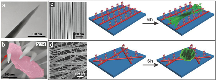
Based on the discovery that the β-lactam-resistant (BLR) bacteria exhibited cell stiffness values nearly 10 × lower than that of β-lactam-susceptible (BLS) bacteria, resulting from decreased peptidoglycan biosynthesis, Wang's group created a model of cellular membrane penetration strains by modulating the tip diameters of NiCo(OH)2CO3 NWs, which had a needle-like shape (Fig. 2a) [69]. The maximum value of free energy density concentrated at the tip of the NW decreases with increasing tip diameter, and the BLR bacteria demonstrated a greater propensity to be captured by the sharpest NWs (Fig. 2b), even with the substrate having been washed three times with deionized water prior to the preparation of the confocal laser scanning microscopy (CLSM) samples, the penetrated BLR bacteria remained immobilized on NWs. This structure has potential applications in the field of biosensing. Moreover, this group used Ag NWs to prepare a highly uniform and long-range ordered array that can be conveniently transferred to any substrate, presenting an ideal membrane for SERS to monitor cell adhesion and development, and to perceive the molecular information of substrate provoked stretch cell growth [70]. The nanowires were observed to be arranged in a side-by-side pattern, displaying 2D ordered structures with a lamellar period of 72.7 ± 4.1 nm (Fig. 2c). The adsorption of extracellular matrix proteins on the oriented Ag NW array is anisotropic (Fig. 2d). Due to the resistance in the stretching direction of the cell body was much smaller than that in the radial direction, the newly formed proteins were transported along the direction of the array, which resulted in the cells growing along the orientation of the oriented array. The results of the SERS spectroscopic analysis demonstrated that the ability of the cell to identify positional cues triggered intracellular signalling pathways.
Layered structures can be divided into single-layer structures and multi-layer structures. The design of a single-layer structure not only considers the shape and size of NPs or NP assemblies but also takes into account the arrangement of NPs or NP components, including their orientation, regularity, and spacing. A multi-layer structure is formed by stacking two or more single-layer structures, so its performance depends not only on the arrangement of single-layer structures but also on the connection and stacking methods between layers. This results in two significant advantages of multi-layers: Firstly, by adding additional layers with specific functions, the sensitivity and selectivity of sensors can be improved. For example, one layer can be designed to specifically identify target molecules or filter out interfering molecules, while another layer acts as a transducer to convert the recognition event into a measurable signal. Secondly, modifying the configuration of one layer can enhance the transmission capability or achieve unique new functions such as spatial separation.
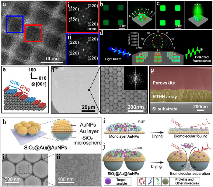
NP assemblies repeat as 2D planar units, which can form single-layer superlattice arrays. In comparison to arbitrarily arranged NPs, long-range-ordered nanocrystal superlattices offer augmented interparticle coupling and a lessening in defects, thereby conferring exceptional electric, optical, and mechanical properties. Wang's group used capillary force to prepare a variety of superlattice structures, including circle, square, pentagon, hexagon, pentagram, and cross arrays by template method [71]. Compared with the traditional NP films, the long-range-ordered superlattice structures exhibit higher electric polarizability, which effectively reduces the cross-impact and improves the transmission efficiency of electrical signals. The achievement of a switchable ferroelectric polarization through the incorporation of azobenzene into superlattice arrays has been made possible. This phenomenon is prompted by the transition between order and disorder of the stacking of nanocrystals during the reversible isomerization process of azobenzene. In addition, this group prepared supercompact SPs with good superlattice domains by thermal controlled-emulsion self-assembly method [72]. Both structures are designed to improve the transmission capacity of photoelectric signals and have potential applications in optical sensing. Recently, Wang's group successfully constructed a superperfect NP superlattice with a simple tetragonal structure and lattice alignment, realizing the transformation from simple cubic to a simple tetragonal crystal structure [49]. The NP superlattice contains the same densely packed perovskite nanocubes, and each superlattice domain can be regarded as a huge single crystal micro cube (Fig. 3a). The uniaxially oriented superperfect component showed previously unrealized precise spatial layout of centimeter, nanometer, and atomic scales, leading to a strong emission burst (Figs. 3b and c). The distance between particles along the z axis is shorter than that along the x and y axes, and the strong coupling effect along the z axis leads to anisotropic optical properties, resulting in NP superlattices showing uniaxial crystal light bodies with directional transition dipoles (Fig. 3d). This structure has a very bright future in the field of fluorescence sensing. Chen et al. have synthesized gold nanopolyhedrons (AuNPH), and subsequently developed flexible AuNPH superlattice sheets as nonconventional SERS platforms [73]. The AuNPHs is closely packed with an average spacing of 6.2 nm. At the macroscopic scale, the sheet can attain a maximum transverse dimension of 0.5 cm, yielding the diameter/thickness aspect ratio of approximately 60,000. The enhanced electromagnetic field is evenly distributed throughout the entirety of the sheet's surface, resulting in an almost uniform SERS signal.
Due to certain limitations in sensing applications, the single-layer structure has been subject to research aimed at further improvement. One of the primary modifications is the generation of sensors with multi-layer structures, which have been widely studied. The 3D volumes were generated by stacking 2D layers onto each other. Koo et al. assembled the Zn-based zeolite imidazole framework (ZIF-8) on Pd NWs to prepare a bilayer H2 gas sensor [74]. Kim et al. used a similar H2 sensor model to cover Pb NPs with a bilayer film composed of poly(methyl methacrylate) (PMMA) and ZIF-8, and PMMA can effectively prevent CO gas molecules from penetrating the sensor [75]. Namgung et al. fabricated a stretchable gas sensor using a bilayer structure formed by nanorods (NRs) and NWs [76]. With synergistic interplay of Al-doped ZnO (AZO) NRs and Ag NWs, the sensor also emerged a high response to NO2 gas under a large strain of 30%. In view of the noninteractive effect between analytes and Raman-active substrates, Wang's group coated the additional perovskite films with specific optical constants on the elongated tetrahexahedral gold nanoparticle (ETHH AuNP) arrays for superficiallayerenhanced Raman scattering (SLERS) detection [55], wherein the array combines layered and hexagonal structures (Figs. 3e–g). The encapsulated perovskite layer could create an effective degree of distance in the vertical Raman-active field when compared to the spin-coating of different medium solutions such as poly(dimethylsiloxane) (PDMS), poly(vinylpyrrolidone) (PVP), and air on an ETHH array.
Furthermore, modifications to the morphology of a given layer can allow for the customization of the sensing properties. Moon et al. coated the metal oxide with Au nanoclusters (AuNCs) with adjustable morphology to analyze the Au-configuration-dependent gas sensing behaviors and the role of AuNCs in gas reforming and oxidation [77]. The uniform coating of AuNCs onto the SnO2 spheres, wherein the majority of the Sn element is evenly dispersed throughout the entirety of the sensing film, and the Au is concentrated on the top layer of the thick film. The overall gas response demonstrated a tendency to rise upon the application of a 0.5 nm thick layer of Au. This trend was further enhanced by increasing the coating thickness up to 1 nm, and reached in the highest response level. It was also discovered that the overall gas responses exhibited a decrease when the duration of annealing was either curtailed or elongated, which provided evidence that gas response is influenced not solely by the quantity of AuNCs but also by the configuration of the AuNCs. In 2022, Wang's group constructed a binary nanosphere array with a trilayer structure through a layer-by-layer assembly strategy (Fig. 3h) [78]. The basal layer was composed of SiO2 spheres exhibiting the opal structure, which presented a periodic distribution of nanopores as a consequence of the hexagonal symmetric arrangement of SiO2 spheres, thereby functioning as a nanoporous membrane. The diameter of the SiO2 spheres could be modified to regulate the pore size. The Au layer at the intermediate position was achieved through the process of magnetron sputtering onto the SiO2 opal plane. The uppermost AuNPs were compactly arranged and distributed across the surface of the SiO2@Au template, which could adhere to target molecules that interact with Au and generate SERS hotspots that offer high intensity and density. In the process of biofluid drying, the analytes interacting with Au are bound to the surface of the substrate, whereas the rest of the non-target substances penetrate into the bottom of the nanosphere to achieve separation (Figs. 3i and j). This trilayer structure reduced the biological pollution of the SERS substrate and the interference of complex components, and effectively retained 57.3% of the original signal after exposure to unprocessed artificial tears under optimal conditions. In addition, this binary nanosphere array was used for tear collection and sensing, which successfully distinguished jaundice patients from 30 clinical cases.
Similar to single-layer structures, the use of single core structures has become insufficient to meet the requirements of complex sample sensing. By contrast, composite structures, such as core-shell structures, have emerged as a more effective option. The core-shell structure not only has the function of coating, but also endows the core particles with specific catalytic activity, electrical, optical, magnetic, and other properties through a special gradient structure. Due to the synergistic effects between different components, shell materials and core materials have been maximally utilized in sensing applications. For example, the presence of the shell can extend the contact time between target molecules and core materials and suppress the decay of the electromagnetic field around the surface of the core metal. Lu et al. developed a general approach to attain the encapsulation of diverse SERS-active NPs within the frameworks [79]. Surfactant-stabilized nanostructured SERS-active NPs with different sizes, shapes and compositions were to be encapsulated by ZIF-8.
Wang's group developed a straightforward yet sensitive electrogenerated chemiluminescence (ECL) biosensing platform to accurately quantify the N6-methyladenine (m6A) RNA sequence [80]. This was achieved through the extinction of luminescent MOFs by ferrocene (Fc) as well as the high complementary characteristic between the m6A antibody and m6A RNA. The encapsulation of the luminophore of Ru(bpy)32+ into the cavities and its adsorption on the MOFs surface was employed, which offered a protracted residence time of ECL indicator on the electrode surface, and remedied the deficiency that Ru(bpy)32+ is conveniently released when used for aqueous-phase detection. Furthermore, the multipore/channel architecture of MOFs can provide a suitable site for pertinent ECL reactions, leading to the significant improvement in both ECL efficiency and stability. Insufficient contact between gaseous analytes and solid substrates may result in a significant portion of the analytes being carried away by the main flow, thereby limiting the adsorption of molecules onto the SERS substrate. In order to slow down the gas flow rate, Wang's group prepared a core-shell SERS substrate, gold superparticles (GSPs)@ZIF-8 particles consisting of a GSPs core and ZIF-8 shell [59]. A single GSP core was surrounded by a shell of ZIF-8 that was approximately 150 nm thick (Fig. 4a). Energy-dispersive X-ray elemental mapping indicated that the Zn exhibited uniform distribution across the entire nanostructure, whereas the Au was found to be concentrated within the core (Figs. 4b–d). The ordered GSPs act as SERS hotspots where gaps between AuNPs in GSP were highly consistent, which caused high-intensity electromagnetic fields. However, the electromagnetic field around the metal/medium (usually air) interfaces will decay sharply, so the addition of a ZIF-8 shell could suppress the attenuation of electromagnetic fields around the GSP surface (Fig. 4e). The presence of the MOF shell also prolonged the contact time between gas molecules and GSPs (Fig. 4f). The SERS signal of p-aminothiophenol (4-ATP) in response to gaseous aldehydes was conspicuous in complex VOCs systems, even down to ppb levels. Wu et al. prepared a core-shell Pt@NiO-based hydrogen gas sensor, which has a higher response than Pt/NiO and NiO to 5000 ppm H2 [81]. Raza et al. prepared tubular core-shell structures by coating the carbon nanotube core [82,83]. Due to the large surface area and low charge recombination rate of CNTs, it provides a suitable conductive platform for metal oxides. However, metal oxides respond highly to analytes and control the size of their constituent shells to demonstrate that the sensor performance is controlled by the ratio of hole accumulation layer thickness to total layer thickness [82].

Based on self-assembled Fmoc dipeptide hydrogels for in situ 3D cell culture, the group used that as a 3D cell culture scaffold to immobilize HeLa cells and two cascade enzymes (CSH-hydrogel) (Figs. 4g and h) [38]. The Fmoc peptide hydrogel is able to furnish a biocompatible environment required for the immobilized enzymes, thereby assuring the retention of enzyme activity. The successful integration of HeLa cells and two enzymes into the matrix have resulted in a confinement effect (Fig. 4i), wherein the enzyme is close to the cells of producing O2•—, the diffusion distance is exceedingly short, resulting in the immediately capture and sensitively detect the released O2•—. Besides that, the restriction of 3D structure of hydrogel and the concentration effect of O2•— make the O2•— have a longer dead time. This may significantly enhance the sensitivity of the sensor.
There are limitations to the use of solid core-shell structures in some existing sensors. One major drawback is that the target molecule usually takes a long time to approach the active NPs within the core. However, there is a potential solution to this problem: hollow structures. Hollow structures with higher specific surface areas allow for better diffusion of analytes, making it easier for them to reach the active site. In addition, controlling the flow state of internal target molecules by the hollow structure can lead to two distinct advantages: the increased contact area between the sensor and analytes to improve sensitivity, and accelerated reaction rates between the sensor and analytes to reduce response time. Therefore, by utilizing hollow structures for sensors, researchers can potentially overcome the limitations associated with solid core-shell structures and improve the overall performance of these types of sensors.
Li et al. synthesized hierarchical hollow ZnO nanocages by using Zn-based metal-organic frameworks (MOF-5) as a precursor, in which the hollow interior was encapsulated by interpenetrating ZnO NPs as porous shells, while the meso-/macro-pore combined channels promoted the diffusion and surface reaction of gas molecules [84]. In the same way, Jang et al. prepared PdO NPs functionalized Co3O4 and SnO2 hollow nanocage by using Co-based zeolite imidazole framework (ZIF-67) as a template for selective detection of acetone molecules [85,86]. Jo et al. adjusted hierarchical nanoarchitectures of Co3O4 nanocages by changing their size, which resulted in high response and selectivity for monitoring xylene, toluene, and methylbenzene [87]. Wang et al. reported a hollow structure based on molecularly imprinted NPs (@MIPs) for the rapid and efficient detection of λ-cyhalothrin in environmental water samples [88].
Wang's group designed hollow nanocages of Co-Ni layered double hydroxide (LDH) on Ag NWs as a means of achieving superior performance through enhanced adsorption of target analytes in the active site of SERS [89]. Bunched polyhedron ZIF-67 NPs were first wrapped on Ag NWs, and then the ZIF-67 framework was decomposed by ion etching to form hollow nanocages with the same size as pristine ZIF-67 template (Fig. 5a). When gas molecules travelled through the porous LDH nanocages, their motion was disturbed, causing them to drift in swirling patterns of flow, oscillating in a bi-directional manner around the centrally placed Ag NWs. The effective diffusivity is proportional to the reciprocal of the square of the geometrical tortuosity. In other words, the higher tortuosity value means a longer, more complex and tortuous path, resulting in greater resistance to fluid flow (Fig. 5b). In the presence of LDH nanocages, the flow will continue to remain irregular and lead to a heightened degree of drag, especially pressure drag, induced by the pressure discrepancy between the anterior and posterior surfaces of the entity due to the entrapment of gaseous molecules within the LDH nanocages. Compared with Ag@ZIF-67, the ability to adsorb and capture gaseous molecules of Ag@LDH got remarkable improvement. In 2022, this group developed a SERS strategy that detects exhalation of breath by using a hollow structure ZIF-8 coated on GSPs [90]. In contrast with GSPs@ZIF-8 (Figs. 5c–f), the interfering gas molecules would not be confined on SERS hotspots of MOF shell with a hollow structure (Figs. 5g and h), thus avoiding interference signals and reduction of detection limit caused by the interfering molecules occupying detection sites. In addition, when gas molecules diffuse slowly and concentrate in the cavity when they pass through porous ZIF materials. The chemical reaction efficiency of target molecules losing kinetic energy and modified molecules is improved, and then more molecules are captured on the surface of the Raman-enhanced SP, thus generating strong Raman signals (Figs. 5i and j). At the same time, interfering molecules cannot be captured by the scaffolding that is 4-ATP was modified on the surface of GSPs, resulting in the non-generation of interfering signals.

The sensing performance of a sensor is greatly affected by the rate of mass transfer across the interface of the intended target. A slower rate of mass transfer can result in a slower rate of interfacial reaction. In order to overcome the limitations of surface diffusion, a concave structure can be designed to generate sudden concentration gradients. A concentration gradient perpendicular to the surface can be generated by surface adsorption in the low concentration area near the sensor surface, which can accelerate the diffusion speed of the target analytes toward the solid sensor surface and reduce the thickness of the stagnant boundary layer near the sensor surface. Additionally, the concave structure can induce vortex phenomena when gas molecules pass through, which can prolong the period of interaction between the gas and the surface. This design can potentially enhance the sensitivity of the sensor.
Wang's group was inspired by the structural characteristics (Fig. 6a) of the moth's antenna, a dendritic Ag nanocrystal substrate (Figs. 6b and c) was prepared to measure aldehydes of the typical lung cancer biomarkers [91]. The multibranched structure in the dendritic Ag nanocrystal generates a considerable number of cavity traps. When the gaseous aldehydes pass through the dendritic structure, the shear layer impacts against the downstream edges of the side branches, and the percolation of air is immediately reversed to the upstream point of impingement (Figs. 6d and e). In other words, when gaseous aldehydes travel across the dendritic surface, the "cavity vortex" phenomenon amplifies the period that the gas interacts with the surface, therefore overcoming the traditional challenge of the poor capability for gaseous molecules to be absorbed on solid substrates. The SERS signal exhibits significant changes, even presenting a detection limit at the ppb level, when the aldehydes bound to dendritic Ag nanocrystals by reaction with Raman active probe molecules.

Since then, this group has also designed micromeshed arrays (Fig. 6f) based on the same structural principle to integrate vertical and horizontal diffusion pathways [92]. It was proposed that a structured setup of the solid reagent be employed to generate a consistent arrangement comprising both reactive and unreactive areas (Fig. 6g). Target analytes adhere to the reactive area and undergo a transformation into products. The reaction areas adsorbed target analytes and converted it into a product, while the unreaction areas did not adsorb analytes and sustained an unchanged surface concentration. The concentration gradients with sudden changes created along the solid reagent's surface expedite the movement of target analytes towards the reactive areas. When used as gas sensors, these arrays constructed of concave structures exhibit a sensitivity level that is an order of magnitude higher than traditional film-based sensors. Moreover, this group used a SiO2 opal array as a substrate to self-assemble AuNPs in the gaps of SiO2 microspheres (Figs. 6h and i) [93]. The surface of citrate-encapsulated AuNPs and calcein connected through the establishment of intermolecular hydrogen bonds, resulting in the assembly of the adjacent AuNPs into a concatemeric configuration. The regulation of the sizes of vertical nanochannels on arrays is achievable through the sizes of SiO2 microspheres, wherein DNA hybridization efficiency is highest at the size of 500 nm of SiO2 microspheres. The microvortex is located in the microcavity situated at the bottom of arrays, which accelerated the transport of analytes to the solid-liquid interface. The collision probability depends on the mass transfer rate of the target analyte, which directly affects the sensitivity of the solid-liquid interface sensor. The AuNP-bridge array has vertical permeability and a microvortex effect compared with the AuNP-planar array, which accelerates the movement of target DNA toward the solid-liquid interface to improve the collision probability between the target DNA and probe DNA, ultimately improving the DNA hybridization efficiency (Figs. 6j–l). Furthermore, the AuNP-bridge array showed fast DNA hybridization kinetics, which acted as a substrate for microRNA-21 detection.
The effective interaction between solid surfaces and analytes in fluids is the first step in promoting continuous recognition, adsorption of analyte, or signal transduction, which is mainly limited by mass transfer or reaction rate. To address the problem of slow diffusion of analytes, shaking, electrothermal flow or microfluidic methods are commonly used to generate advection to bring fresh analytes near the active surface. In recent years, with significant advancements made by researchers in developing new technologies and applications, deformable structures have gained increasing attention. These types of structures are unique in that they can bend, twist, and flex to adapt to their surroundings. Unlike static structures that cannot move, deformable structures are capable of adjusting their shape according to external forces. The mass transfer can also be effectively promoted by designing surfaces with deformable structures, which is mainly due to the rapid movement of reactants on the surface caused by the dynamic deformation of nanostructures, as well as the vortices generated by the convection around the surface.
Wang's group has achieved noteworthy success in the design of deformable structures. Inspired by the natural trapping process of the Venus flytraps, they prepared a deformable NW in which the tip region of the polycrystalline NW bends easily when dragged by the molecular force of the ligand-receptor, thereby forming a nanoclaw [94]. The nanowires have a comparatively low Young's modulus, which permitted them to undergo elastic deformation and assume a bent shape (Fig. 7a). Upon contact with the nanowire arrays, the target bacteria promptly triggered the bending of the initially soft and straight nanowires, resulting in the closure of the trap (Fig. 7b). The deformation of nanowires was initiated by the robust adhesive force of bacteria, which was potent enough to forestall the trapped bacteria from fleeing. The efficiency of bacterial capture by the 3D nanoclaws surpassed that by rigid nanowire arrays with a factor of two. Therefore, this structure may have potential applications in biosensing. Le Saux et al. reported the development of antigen-functionalized ZnO NWs-driven system that enables efficient detection and monitoring of cellular forces [95]. In this system, natural killer (NK) cells exert a centripetal force on the NWs, which stimulate cell contraction, causing the NWs to bend. The cells apply forces as low as 10 pN, based on NWs deformation analysis.

In addition, Wang's group constructed two deformable nanosheets. One is a deformable MOF nanosheet [96], which can alter its shape in response to fluid variation, similar to the swaying of coral in the ocean (Figs. 7c–g). When subjected to shear stress by fluids, flexible nanosheets undergo nonlinear deformation as a result of difference in stiffness distribution. The swaying of flexible nanosheets generation of robust vortices (Fig. 7d), whereas neither the rigid nor the bulk-type nanosheets produced any vortex. Shear stresses were generated as the fluid moves along the MOF surface, resulting in a flow velocity close to zero at the bottom of the nanosheet and an increase in the flow velocity at the edge region (Fig. 7e). Compared with the purely diffusive process observed in laminar flow, it is noted that the convective transport phenomenon induced by a vortex can lead to a notable enhancement of reactant transport. The vertical flow between the flexible nanosheets led to the downward transportation of the reaction components and consequently produced a concentration field that is more uniform in comparison to the situation where the bulk case or the rigid nanosheets were used. Thus, deformable flexible nanosheets break the slow molecular diffusion stagnation layer that inhibits rapid contact between reactants and heterogeneous catalysts to facilitate mass transport to the catalyst surface. Compared with the system containing nondeformable MOFs, deformable MOFs can increase dye adsorption and catalytic conversion by a factor of five and three, respectively. This structure overcomes the limitations of surface diffusion and has potential applications in designing sensors that detect trace analytes to improve sensitivity. For example, based on the flexibility feature that can improve analyte-solid interface interaction and promote mass transfer, Cao et al. used the flexibility of M13 bacteriophages to prepare nanointerfaces with deformable structures that have both the functions of capturing pathogens and sensing [97]. During the process of pathogen capture, M13 nanofibers that are adorned with multivalent ligands function in a similar manner to the tentacles of an octopus with numerous suction cups. Such properties of flexibility and extensibility can enhance the chance of the ligand contacting the target. During the process of sensing, the M13 nanofibers exhibit swaying motion similar to that of coral being influenced by the flow of the ocean. This facilitates the diffusion of more c-apt molecules into the solution, thereby preventing them from attaching indiscriminately to either the surface of M13 or the microbeads. Compared to free DNA strands, the sensitivity of sensors based on this structure is increased by three orders of magnitude.
Another deformable nanosheet is NF (nickel foam)-CoNiS5 h, which also acquires deformable properties through its low Young's modulus [98]. The NF-CoNiS5 h demonstrated bending behavior under the application of an applied electric field. This gave rise to periodic changes in both deflection angles and displacements, leading to periodic expansion and contraction of the entire material. The deformation of the material not only accelerated the separation of bubbles, but also the forced convection caused by it reduced the concentration gradient, thereby improving the mass transfer of reactants and products around the material. In rigid materials, the gaseous product adhered to the surface and underwent a gradual increase in size, ultimately resulting in the formation of larger bubbles. In cases where attachment to the bubbles was hampered by inadequate material adhesion, they were dislodged from the electrode surface. However, in deformable materials, the bubbles are smaller and separate faster. The adhesion of a gaseous bubble onto the solid electrode obstructs water from contacting with the catalyst. Thus, the efficiency of oxygen evolution reaction (OER) is reduced as a result of the formation of inactive catalytic sites under the footprint of gas bubbles. This structure has potential applications in electrochemical sensing.
Drawing inspiration from the fact that the flexibility of polymer ligands can effectively prevent protein adsorption, Wang's group fabricated ultrathin Gd2O3 nanocoils with a low Young's modulus [99], demonstrating that exhibit a feature of transformability when in solution (Fig. 7h). The ultrathin nanocoils were found to be amorphous and lacked structural rigidity, yet their distinctive geometry and noncrystalline character permitted them to be pliable, so that they could twist and pivot within a liquid, analogous to a flag swaying in the breeze (Figs. 7i and j). The level of nonspecific bovine serum albumin (BSA) adsorption on transformable ultrathin nanocoils was considerably less than that on NPs, nanotripods, nanotriangles, and nanodisks. The nanocoils exhibited alterations in their spatial configuration in a solution whereby the augmented steric hindrance repressed nonspecific protein adhesion. Furthermore, the deformable nanocoils displayed steric repulsion and internalization by cells, thus increasing their biocompatibility. The ultrathin gadolinium oxide nanocoils have been verified to effectively extend the image enhancement time through vivo magnetic resonance imaging experiments. This deformable structure can be used in fluorescence-based biosensing.
In chip-based sensors, the interface heterogeneous reaction between sensing materials and analytes is a major obstacle to achieving high sensitivities. This problem can be solved by constructing a reasonable micro/nano structure of the sensing interface. Considering the diversity and application needs of micro/nano structures, multiple preparation strategies should be adopted. With the diverse micro- and nano-structures of sensing materials, chip-based sensors have the potential to enrich, capture, differentiate, and screen biological markers, which allows for early disease diagnosis.
Benefiting from the advance in the interfacial micro- and nano-structures, different processing techniques have been developed for sensing materials with micro- and nano-structures. For the six micro- and nano-structures mentioned above, their preparation methods were briefly described.
Wire structures. Needle-shaped NWs can be obtained by acid etching, and the etching time is varied to control the tip diameter [69]. For the preparation of highly uniform, long-range-ordered Ag NWs, the use of liquid substrates can improve the convection velocity of the Ag NW suspension and complete ordered assemblies [70].
Layered structures. Single-layer structures are mainly prepared by assembly methods, such as solvent evaporation [49], template induction [71], DNA recognition, external field modulation, constrained assembly [100], and synergistic assembly. Multilayer structures are mainly prepared by assembly, deposition [77], and coating methods [55] on the basis of the formed single layer.
Core-shell structures. Shell material growth onto the core can be manipulated by hydrophilic-hydrophilic interaction, electrostatic interactions, and lattice matching. The main methods for preparing nanomaterials with core-shell structure include seeded-growth, sol–gel, hydrothermal, galvanic replacement, microemulsion fusion, redox-coprecipitation, and self-assembly [101].
Hollow structures. Construction of hollow structures can be achieved through two methods: template assisted [102] and template free [103]. The former can be divided into hard-templated, soft-templated, and self-templated methods according to the use of template sources. Template-free method does not require any sacrifice template, which is based on the spontaneous hierarchical assembly of solution to form core-shell structures.
Concave structures. Construction of concave structures can be achieved through both template induction and photolithography. The former refers to the growth or assembly of NPs on the template, and ultimately the overall material has a concave structure [91,93]. The latter refers to the use of photolithography technology to create the desired shape and etching the concave through chemical or physical etching [92].
Deformable structures. Reducing the Young's modulus of nanomaterials by debugging the reaction conditions, which can achieve the purpose of deformability in a fluid environment [94,99]. The flexibility of the living organisms or intelligent materials can be used to create a dynamic deformable nanointerface [97].
In addition, there are various processing technologies, such as electrochemical processing, laser processing, nanoimprinting, and printing, can also be used for micro- and nano-structures. Each method has its unique advantages to achieve specific composition and morphology. The development and joint application of micro- and nano-processing technology provide rich solutions for the combination of multiple structures and the construction of complex structures.
Reasonable design of the micro- and nano-structure of sensing materials can overcome defects caused by interface solid-liquid heterogeneous reactions, such as low sensitivity. Design microfluidic chips with specific micro- and nano-structures will lead to the invention of miniaturized platforms with many advantageous characteristics, such as high sensitivity, low reagent consumption, portability, and disposability. Zhu et al. integrated the hierarchical hydrogel system with ordered micro- and nano-structures into a multichannel concentration gradients microfluidic chip for functional liver cancer-on-a-chip construction and drug screening with good repeatability and high accuracy [104]. Yan et al. integrated a hierarchical structure, the "Rhipsalis (Cactaceae)"-like micropillar array, into the 3D microfluidic chip for capturing cancer cells [105]. Singh et al. demonstrated an ultrasensitive microfluidic biochip with single-layer structural microporous manganese-reduced graphene oxide for detection of cardiac biomarker [106]. The thin layer was produced on the surface of a patterned substrate made of indium tin oxide, and combined with a microfluidic system.
The design of interfacial micro- and nano-structures as an important design strategy is valuable for achieving efficient detection of target ions, molecules, etc., in chip-based sensors, and will also promote the development of new principles and methods in sensing. In this review, we discuss the effect of micro-nano structure design such as wire structures, layered structures, core-shell structures, hollow structures, concave structure and deformable structures on the performance of sensors including chemiresistors, electrochemical sensors, fluorescence sensors, and SERS sensors (Table 1). To further develop micro- and nano-structures for more sensitive, specific, rapid and integrated in chip-based sensors, we propose here three design directions to meet future assay needs.
 DownLoad:
CSV
DownLoad:
CSV

|
Ordered design of surface and interfaces for micro- and nano-structures. The key to achieving efficient target identification, facilitated charge transfer, and stable material transport is to obtain sensing surfaces and interfaces with well-defined, stable, region-specific, and function-specific structures, which requires the ordered design of sensing units such as atoms, molecules, and nanoparticles at the surface and interfaces.
Flexible design of micro- and nano-structures. Flexible sensing devices enable efficient capture of target molecules, increased effective contact area, improved mass transfer, and adaptation to the deformation requirements of detection devices in different operating environments. The flexible design of micro- and nano-structures for detection chips requires addressing the reliability and durability of flexible structures as they are often subjected to repeated bending and stretching.
Multi-functional integrated design of micro- and nano-structures. The multifunctional integrated design of micro- and nano-structures has the following two characteristics: the multifunctional integrated design technology can integrate multiple separation and analysis detection technologies into the same platform, thus reducing the time and cost of analysis and detection; the multifunctional integrated design technology can realize multiple detection of the same sample, thus improving the accuracy and reliability of analysis and detection.
Chip-based detection based on micro- and nano-structures need theories and methods from many fields such as mathematics, physics, chemistry and biology to analyze, detect, identify and measure matter, energy and information, which can achieve efficient detection, miniaturization and integration. It will play an increasingly important role in medical diagnosis due to the ability to solve the problem of low sensitivity caused by interface liquid-solid heterogeneous reactions. Currently, portable detection devices used for human physical indicator testing only serve as medical aids and do not meet the requirements of medical diagnosis. In addition to the solution to the sensitivity problem mentioned above, combining printing and NP assembly can address unstable signal resulting from uneven quality and poor repeatability of sensing materials. Establishing a universal detection mechanism can address the complexity of multiple sensing mechanisms, such as the difference in ideal operating temperature caused by the integration of multiple sensing elements on the chip (Fig. 8). The transformation from traditional detection to real-time online detection is an inevitable trend in the development of medical diagnosis, which includes material design, mechanism research, chip processing, instrument development, and clinical testing. Therefore, interdisciplinary research will be beneficial for the commercialization of chip for detection.

The authors declare no competing financial interest.
This work was financially supported by the National Natural Science Foundation of China (No. 21925405).
Supplementary material associated with this article can be found, in the online version, at doi:
L. Xue, H. Yamazaki, R. Ren, et al., Nat. Rev. Mater. 5 (2020) 931–951. doi: 10.1038/s41578-020-0229-6
C.I.L. Justino, A.R. Gomes, A.C. Freitas, A.C. Duarte, T.A.P. Rocha-Santos, Trends Anal. Chem. 91 (2017) 53–66. doi: 10.1016/j.trac.2017.04.003
A.A. Nayl, A.I. Abd-Elhamid, A.Y. El-Moghazy, et al., Trends Environ. Anal. 26 (2020) e00087. doi: 10.1016/j.teac.2020.e00087
D. Marzorati, L. Mainardi, G. Sedda, et al., Chemosensors 9 (2021) 209. doi: 10.3390/chemosensors9080209
X.Y. Zhou, Z.J. Xue, X.Y. Chen, et al., J. Mater. Chem. B 8 (2020) 3231–3248. doi: 10.1039/c9tb02518a
S. Freddi, A.V. Emelianov, I.I. Bobrinetskiy, et al., Adv. Healthcare Mater. 9 (2020) 2000377. doi: 10.1002/adhm.202000377
M.A. Boles, M. Engel, D.V. Talapin, Chem. Rev. 116 (2016) 11220–11289. doi: 10.1021/acs.chemrev.6b00196
Z.M. Wang, R.B. Yu, Adv. Mater. 31 (2019) 1800592. doi: 10.1002/adma.201800592
J. Park, Y. Lee, J. Hong, et al., ACS Nano 8 (2014) 12020–12029. doi: 10.1021/nn505953t
Y.B. Zhang, K.F. Chan, B. Wang, P.W.Y. Chiu, L. Zhang, Sens. Actuator. B: Chem. 271 (2018) 128–136. doi: 10.3390/ijerph15010128
S.Q. Song, C.F. Zhang, W.Z. Li, et al., Nano Energy 100 (2022) 107513. doi: 10.1016/j.nanoen.2022.107513
N.N. Bai, L. Wang, Q. Wang, et al., Nat. Commun. 11 (2020) 209. doi: 10.1038/s41467-019-14054-9
C. Zhang, M.L. Qu, X.Q. Fu, J. Lin, Small Methods 6 (2022) 2101384. doi: 10.1002/smtd.202101384
A.L. Rogach, Angew. Chem. Int. Ed. 43 (2004) 148–149. doi: 10.1002/anie.200301704
P. Song, Y. Wang, Y. Wang, et al., J. Am. Chem. Soc. 137 (2015) 3069–3075. doi: 10.1021/ja5127903
S. Guo, S. Dong, J. Mater. Chem. 21 (2011) 16704–16716. doi: 10.1039/c1jm11382h
L. Wang, L. Xu, H. Kuang, C. Xu, N.A. Kotov, Acc. Chem. Res. 45 (2012) 1916–1926. doi: 10.1021/ar200305f
S. Ohta, D. Glancy, W.C.W. Chan, Science 351 (2016) 841–845. doi: 10.1126/science.aad4925
T. Bao, Y. Zou, C. Zhang, C. Yu, C. Liu, Angew. Chem. Int. Ed. 61 (2022) e202209433. doi: 10.1002/anie.202209433
S. Bhogal, K. Kaur, A.K. Malik, et al., Trends Anal. Chem. 133 (2020) 116043. doi: 10.1016/j.trac.2020.116043
S. Freddi, M.C.R. Gonzalez, P. Carro, L. Sangaletti, S.D. Feyter, Angew. Chem. Int. Ed. 61 (2022) e202200115. doi: 10.1002/anie.202200115
J. Dai, O. Ogbeide, N. Macadam, et al., Chem. Soc. Rev. 49 (2020) 1756–1789. doi: 10.1039/c9cs00459a
M.J. Bezdek, S.X.L. Luo, R.Y. Liu, Q.L. He, T.M. Swager, ACS Cent. Sci. 7 (2021) 1572–1580. doi: 10.1021/acscentsci.1c00746
H.Y. Li, S.N. Zhao, S.Q. Zang, J. Li, Chem. Soc. Rev. 49 (2020) 6364–6401. doi: 10.1039/c9cs00778d
H.J. Kim, J.H. Lee, Sens. Actuators. B: Chem. 192 (2014) 607–627. doi: 10.1016/j.snb.2013.11.005
V. Schroeder, S. Savagatrup, M. He, S. Lin, T.M. Swager, Chem. Rev. 119 (2019) 599–663. doi: 10.1021/acs.chemrev.8b00340
B. de Lacy Costello, A. Amann, H. Al Kateb, et al., J. Breath Res. 8 (2014) 014001. doi: 10.1088/1752-7155/8/1/014001
B. Crone, A. Dodabalapur, A. Gelperin, et al., Appl. Phys. Lett. 78 (2001) 2229–2231. doi: 10.1063/1.1360785
R. Song, X. Zhou, Z. Wang, et al., Org. Electron. 91 (2021) 106083. doi: 10.1016/j.orgel.2021.106083
S.J. Kim, S.J. Choi, J.S. Jang, et al., Adv. Mater. 29 (2017) 1700737. doi: 10.1002/adma.201700737
H. Shin, D.H. Kim, W. Jung, et al., ACS Nano 15 (2021) 14207–14217. doi: 10.1021/acsnano.1c01350
C. Sun, G. Feng, Y. Song, et al., Anal. Chem. 94 (2022) 6615–6620. doi: 10.1021/acs.analchem.2c00897
C. Sun, R. Li, Y. Song, et al., Anal. Chem. 93 (2021) 6188–6194. doi: 10.1021/acs.analchem.1c00372
C. Sun, M.V. Vinayak, S. Cheng, W. Hu, Anal. Chem. 93 (2021) 11305–11311. doi: 10.1021/acs.analchem.1c02601
L. Fan, J.J. Huang, J. Liao, Sens. Actuator. B: Chem. 369 (2022) 132164. doi: 10.1016/j.snb.2022.132164
T. Sierra, I. Jang, E. Noviana, et al., ACS Sens. 6 (2021) 2998–3005. doi: 10.1021/acssensors.1c00864
S. Ramalingam, A. Elsayed, A. Singh, Mikrochim. Acta 187 (2020) 645. doi: 10.1007/s00604-020-04589-w
M.L. Lian, L. Xu, X.W. Zhu, et al., Anal. Chem. 89 (2017) 12843–12849. doi: 10.1021/acs.analchem.7b03371
Y. Wang, H. Feng, H. Zhang, et al., Analyst 145 (2020) 1294–1301. doi: 10.1039/C9AN02390A
Y. Zhou, H. Yin, W.W. Zhao, S. Ai, Coordin. Chem. Rev. 424 (2020) 213519. doi: 10.1016/j.ccr.2020.213519
R. Pandey, Y. Lu, E.M. McConnell, et al., Biosens. Bioelectron. 224 (2023) 114983. doi: 10.1016/j.bios.2022.114983
R. Pandey, D. Chang, M. Smieja, et al., Nat. Chem. 13 (2021) 895–901. doi: 10.1038/s41557-021-00718-x
Y. Xu, W. Huang, Y. Zhang, H. Duan, F. Xiao, Anal. Chem. 94 (2022) 4463–4473. doi: 10.1021/acs.analchem.1c05544
L. Basabe-Desmonts, D.N. Reinhoudt, M. Crego-Calama, Chem. Soc. Rev. 36 (2007) 993–1017. doi: 10.1039/b609548h
K. Liu, C. Shang, Z. Wang, et al., Nat. Commun. 9 (2018) 1695. doi: 10.1038/s41467-018-04119-6
X. Chen, K. Xu, J. Li, et al., Biosens. Bioelectron. 155 (2020) 112104. doi: 10.1016/j.bios.2020.112104
M.Y. Liu, Z. Gao, Y.J. Yu, et al., Nanoscale Res. Lett. 13 (2018) 27. doi: 10.1186/s11671-018-2440-6
H. Eskandari, M. Amirzehni, H. Asadollahzadeh, J. Hassanzadeh, P.A. Eslami, Sens. Actuator. B: Chem. 275 (2018) 145–154. doi: 10.1016/j.snb.2018.08.050
X. Li, Z.J. Xue, X.Y. Chen, et al., Sci. Adv. 11 (2022) eadd1559.
Y. Shi, Y. Hu, N. Jiang, A.K. Yetisen, ACS Sens. 7 (2022) 1615–1633. doi: 10.1021/acssensors.2c00313
S. Wang, L. Zheng, G. Cai, et al., Biosens. Bioelectron. 140 (2019) 111333. doi: 10.1016/j.bios.2019.111333
M. Meeseepong, G. Ghosh, S. Shrivastava, N.E. Lee, ACS Appl. Mater. Interfaces 15 (2023) 21754–21765. doi: 10.1021/acsami.2c22352
S.Y. Ding, E.M. You, Z.Q. Tian, M. Moskovits, Chem. Soc. Rev. 46 (2017) 4042–4076. doi: 10.1039/C7CS00238F
M.F. Cardinal, E. Vander Ende, R.A. Hackler, et al., Chem. Soc. Rev. 46 (2017) 3886–3903. doi: 10.1039/C7CS00207F
X.Z. Qiao, Z.J. Xue, L. Liu, K.Y. Liu, T. Wang, Adv. Mater. 31 (2019) 1804275. doi: 10.1002/adma.201804275
F. Sun, H.C. Hung, A. Sinclair, et al., Nat. Commun. 7 (2016) 13437. doi: 10.1038/ncomms13437
Y.C. Kao, X. Han, Y.H. Lee, et al., ACS Nano 14 (2020) 2542–2552. doi: 10.1021/acsnano.0c00515
D. Cialla-May, X.S. Zheng, K. Weberabc, J. Popp, Chem. Soc. Rev. 46 (2017) 3945–3961. doi: 10.1039/C7CS00172J
X.Z. Qiao, B.S. Su, C. Liu, et al., Adv. Mater. 30 (2018) 1702275. doi: 10.1002/adma.201702275
S. Hu, Y. Jiang, Y. Wu, et al., ACS Appl. Mater. Interfaces 12 (2020) 55324–55330. doi: 10.1021/acsami.0c12988
J. Guo, F. Zeng, J. Guo, X. Ma, J. Mater. Sci. Technol. 37 (2020) 96–103. doi: 10.1016/j.jmst.2019.06.018
K. Yang, S. Zong, Y. Zhang, et al., ACS Appl. Mater. Interfaces 12 (2020) 1395–1403. doi: 10.1021/acsami.9b19358
L. Ma, S. Ye, X. Wang, J. Zhang, ACS Sens. 6 (2021) 1392–1399. doi: 10.1021/acssensors.1c00063
C.H. Huang, A.L. Li, X.Y. Chen, T. Wang, Small 16 (2020) e2004802. doi: 10.1002/smll.202004802
I. Paulowicz, V. Hrkac, S. Kaps, et al., Adv. Electron. Mater. 1 (2015) 1500081. doi: 10.1002/aelm.201500081
O. Lupan, V. Postica, N. Ababii, et al., Microelectron. Eng. 164 (2016) 63–70. doi: 10.1016/j.mee.2016.07.008
L. Chow, O. Lupan, H. Heinrich, G. Chai, Appl. Phys. Lett. 94 (2009) 163105. doi: 10.1063/1.3118583
S. Wei, Z. Li, K. Murugappan, et al., Adv. Mater. 35 (2022) 2207199.
L.Z. Liu, S. Chen, X. Zhang, et al., Sci. Adv. 6 (2020) eabb9593. doi: 10.1126/sciadv.abb9593
Z. Zhang, Y. Fu, W. Yu, et al., Adv. Mater. 28 (2016) 9589–9595. doi: 10.1002/adma.201603223
J.G. Feng, Q. Song, B. Zhang, et al., Adv. Mater. 29 (2017) 1703143. doi: 10.1002/adma.201703143
D. Luo, X.Y. Qin, Q. Song, et al., Adv. Funct. Mater. 27 (2017) 1701982. doi: 10.1002/adfm.201701982
Y. Chen, H.J. Yin, D. Sikdar, et al., ACS Appl. Nano Mater. 4 (2021) 12498–12505. doi: 10.1021/acsanm.1c02884
W.T. Koo, S. Qiao, A.F. Ogata, et al., ACS Nano 11 (2017) 9276–9285. doi: 10.1021/acsnano.7b04529
H. Kim, W. Kim, S. Cho, J. Park, G.Y. Jung, ACS Appl. Mater. Interfaces 12 (2020) 28616–28623. doi: 10.1021/acsami.0c05369
G. Namgung, Q.T.H. Ta, W. Yang, J.S. Noh, ACS Appl. Mater. Interfaces 11 (2019) 1411–1419. doi: 10.1021/acsami.8b17336
Y.K. Moon, S.Y. Jeong, Y.C. Kang, J.H. Lee, ACS Appl. Mater. Interfaces 11 (2019) 32169–32177. doi: 10.1021/acsami.9b11079
W.D. Zhao, J.M. Li, Z.J. Xue, et al., Angew. Chem. Int. Ed. 61 (2022) e202205628. doi: 10.1002/anie.202205628
G. Lu, S. Li, Z. Guo, et al., Nat. Chem. 4 (2012) 310–316. doi: 10.1038/nchem.1272
W.Q. Bai, A.P. Cui, M.Z. Liu, et al., Anal. Chem. 91 (2019) 11840–11847. doi: 10.1021/acs.analchem.9b02569
C.H. Wu, Z. Zhu, H.M. Chang, et al., J. Alloys Compd. 814 (2020) 151815. doi: 10.1016/j.jallcom.2019.151815
M.H. Raza, K. Movlaee, S.G. Leonardi, et al., Adv. Funct. Mater. 30 (2020) 1906874. doi: 10.1002/adfm.201906874
M.H. Raza, R. Di Chio, K. Movlaee, et al., ACS Appl. Mater. Interfaces 14 (2022) 22041–22052. doi: 10.1021/acsami.2c00808
W.H. Li, X.F. Wu, N. Han, et al., Sens. Actuator. B: Chem. 225 (2016) 158–166. doi: 10.1016/j.snb.2015.11.034
W.T. Koo, S. Yu, S.J. Choi, et al., ACS Appl. Mater. Interfaces 9 (2017) 8201–8210. doi: 10.1021/acsami.7b01284
J.S. Jang, W.T. Koo, S.J. Choi, I.D. Kim, J. Am. Chem. Soc. 139 (2017) 11868–11876. doi: 10.1021/jacs.7b05246
Y.M. Jo, T.H. Kim, C.S. Lee, et al., ACS Appl. Mater. Interfaces 10 (2018) 8860–8868. doi: 10.1021/acsami.8b00733
J. Wang, H. Qiu, H. Shen, et al., Biosens. Bioelectron. 85 (2016) 387–394. doi: 10.1016/j.bios.2016.05.041
X.Z. Qiao, X.Y. Chen, C.H. Huang, et al., Angew. Chem. Int. Ed. 58 (2019) 16523–16527. doi: 10.1002/anie.201910865
A.L. Li, X.Z. Qiao, K.Y. Liu, W.Q. Bai, T. Wang, Adv. Funct. Mater. 32 (2022) 2202805. doi: 10.1002/adfm.202202805
Z. Zhang, W. Yu, J. Wang, et al., Anal. Chem. 89 (2017) 1416–1420. doi: 10.1021/acs.analchem.6b05117
L. Liu, W. Xiong, L.F. Cui, et al., Angew. Chem. Int. Ed. 59 (2020) 15953–15957. doi: 10.1002/anie.202006408
X.B. Huang, W.D. Zhao, X.Y. Chen, et al., J. Am. Chem. Soc. 144 (2022) 17533–17539. doi: 10.1021/jacs.2c06623
L.Z. Liu, S. Chen, Z.J. Xue, et al., Nat. Commun. 9 (2018) 444. doi: 10.1038/s41467-018-02879-9
G. Le Saux, N. Bar Hanin, A. Edri, et al., Adv. Mater. 31 (2019) e1805954. doi: 10.1002/adma.201805954
C.H. Huang, Z.H. Guo, X. Zheng, et al., J. Am. Chem. Soc. 142 (2020) 9408–9414. doi: 10.1021/jacs.0c02272
Y. Cao, N. Wu, H.D. Li, et al., Small 18 (2022) e2203962. doi: 10.1002/smll.202203962
X.Z. Qiao, X.M. Yin, L. Wen, et al., Chem 8 (2022) 1–11. doi: 10.1016/j.chempr.2021.12.020
D. Luo, S. Cui, Y. Liu, et al., J. Am. Chem. Soc. 140 (2018) 14211–14216. doi: 10.1021/jacs.8b08118
J. Zhang, X. Li, Y. Liu, et al., Adv. Mater. 34 (2022) e2202119. doi: 10.1002/adma.202202119
H. Zou, Z. Luo, X. Yang, Q. Xie, Y. Zhou, J. Mater. Sci. 57 (2022) 10912–10942. doi: 10.1007/s10853-022-07328-z
W.T. Koo, J.H. Cha, J.W. Jung, et al., Adv. Funct. Mater. 28 (2018) 1802575. doi: 10.1002/adfm.201802575
Z.J. Xue, P.L. Wang, A.D. Peng, T. Wang, Adv. Mater. 31 (2019) 1801441. doi: 10.1002/adma.201801441
L. Zhu, C. Shao, H. Chen, Z. Chen, Y. Zhao, Research 2021 (2021) 9845679.
S. Yan, X. Zhang, X. Dai, et al., ACS Appl. Mater. Interfaces 8 (2016) 33457–33463. doi: 10.1021/acsami.6b11673
N. Singh, M.A. Ali, P. Rai, et al., ACS Appl. Mater. Interfaces 9 (2017) 33576–33588. doi: 10.1021/acsami.7b07590

Figure 1 (a) Micro- and nano-structures. (b) Chemiresistive sensing. (c) Electrochemical sensing. (d) Fluorescence sensing. (e) SERS sensing.

Figure 2 (a) TEM images of NiCo(OH)2CO3 NWs with tip diameters of 5 nm. (b) SEM images of BLR Salmonella captured on NW substrata. Reproduced with permission [69]. Copyright 2020, American Association for the Advancement of Science. (c, d) SEM images of oriented Ag NW arrays and random Ag NW films, and schematic illustration of cell adhesion and growth on them respectively. Reproduced with permission [70]. Copyright 2016, John Wiley and Sons.

Figure 3 (a) HR-TEM images of adjacent local NPs in superlattices. (b, c) PL microscopy images of random nanocube aggregates and simple tetragonal phase nanocube superlattices in pixels. (d) Schematic of the identical strong coupling along the z axis of crystalline superlattice array-induced polarized light emission along z axis. Reproduced with permission [49]. Copyright 2022, American Association for the Advancement of Science. (e) Geometric models of atomic arrangements. (f) Low- and high-magnification SEM image of ETHH NP arrays. (g) Cross-sectional SEM images. Reproduced with permission [55]. Copyright 2019, John Wiley and Sons. (h) Schematic and SEM image. (i, j) Schematic diagram of separation for substances in tear on monolayer AuNPs and SiO2@Au@AuNPs substrate. Reproduced with permission [78]. Copyright 2022, John Wiley and Sons.

Figure 4 (a) SEM images of GSPs@ZIF-8. (b-d) Energy-dispersive X-ray elemental mapping of GSPs@ZIF-8. (e) Hotspots in GSPs and GSPs@ZIF-8 around the edges of the plasmon. (f) Schematic illustration of GSPs and GSPs@ZIF-8 with gas collisions. Reproduced with permission [59]. Copyright 2018, John Wiley and Sons. (g, h) SEM image of CSH-hydrogel. (i) Scheme showing the path of O2•− detection in cells cultured in the SH-hydrogel (3D cell culture). Reproduced with permission [38]. Copyright 2017, American Chemical Society.

Figure 5 (a) Diagram of the synthetic route and structure of the nanocage. i-iii) TEM image of Ag NW, Ag@ZIF-67, and Ag@LDH. (b) Simulation streamline chart. Reproduced with permission [89]. Copyright 2019, John Wiley and Sons. (c, g) Schematic diagram of structure, (d, h) TEM images, (e, i) SERS spectra of 4-ethylbenzaldehyde reacted with a substrate, (f, j) schematic diagram of adsorption between exhaled gas molecules and different substrates of GSPs@ZIF‐8 and GSPs@H‐ZIF‐8. Reproduced with permission [90]. Copyright 2022, John Wiley and Sons.

Figure 6 (a) The photo of silkmoth Bombyx mori's antennae. Inset: a silkmoth Bombyx mori. (b, c) High-resolution SEM and TEM image of the dendritic Ag nanocrystals. (d) Velocity magnitude and flow pattern gained from ANSYS 14.5 CFD software. (e) Sketches of the cavity flow dynamics. Reproduced with permission [91]. Copyright 2017, American Chemical Society. (f) Fluorescence micrographs of patterned sensors. (g) Gaseous molecular movement at the interface of patterned arrays. Reproduced with permission [92]. Copyright 2020, John Wiley and Sons. (h, i) SEM images of AuNP-bridge arrays. (j) COMSOL simulation results show the motion rate of the target analyte near the interface of the AuNP-planar and AuNP-bridge arrays. (k, l) DNA molecule movement and hybridization at the solid-liquid interface of the AuNP-planar and AuNP-bridge arrays. Reproduced with permission [93]. Copyright 2022, American Chemical Society.

Figure 7 (a) SEM image of polycrystalline nanowires during bacterial capture. (b) Bacterial capture by 3D nanoclaws at high flow velocity. Reproduced with permission [94]. Copyright 2018, Nature Publishing Group. (c) Cross-sectional SEM images of the as-synthesized MOF nanosheet-assembled frames. (d) Concentration field of reactants on the surface of the flexible nanosheets. (e) Flow field around the flexible nanosheets and the fast movement of reactants on the surface. (f) TEM image of the edge of the MOF nanosheet-assembled frame film. (g) In situ TEM was used to observe the dynamic deformation of the nanosheets at the edge of the NAF film in the fluid. Reproduced with permission [96]. Copyright 2020, American Chemical Society. (h) Schematic representation of adsorption of BSA on a nanocoil. (i) TEM image of ultrathin nanocoils. (j) Liquid TEM images show the transformable property of nanocoils. Reproduced with permission [99]. Copyright 2018, American Chemical Society.
Table 1. Performance, structure design, and applications of sensing micro- and nano-structures.
|
|
 下载: 导出CSV

 扫一扫看文章

扫一扫关注我们

 下载:
下载: