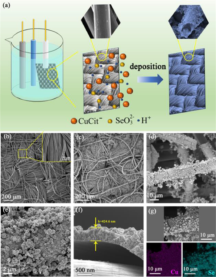
Figure 1.
(a) Schematic illustration of the electrodeposition process. SEM surface observation of (b) carbon clothes and (c-e) Cu2Se@C thin film. (f) The morphology of cross-section and (g) EDS elemental mapping of Cu2Se@C.
Cu2Se@C thin film with three-dimensional braided structure as a cathode material for enhanced Cu2+ storage
Wenhao Chen , Muxuan Wu , Han Chen , Lue Mo , Yirong Zhu

In the face of multiple challenges resulting from the global climate and environmental changes, developing clean energy should be placed at the core of new environmental protection policy. Updating the green energy storage equipment and system is an important way to achieve carbon peak and carbon neutrality. Lithium-ion batteries (LIBs) with high operating voltage, large specific capacity and superior energy density have experienced explosive growth in recent years [1–3]. However, the shortcomings of LIBs such as security issue, low lithium reserves and high cost make it difficult to satisfy the comprehensive industrial standards [4,5]. Compared with batteries with organic electrolyte, aqueous batteries have become the research hotspot owing to their advantages of high ionic conductivity, environmental friendliness and low cost [6–11]. What is more, the use of multivalent charge carrier (Zn2+, Cu2+) can enhance the charge and discharge efficiency.
Recently, cost-effective transition metal oxides and chalcogenides, such as Bi2O2Se [12], MoS2 [13], Sb2Se3 [14], have become the competitive candidate electrode materials for energy storage devices due to their advantages of the variety of structures and morphologies, admirable electronic conductivity, variable valences states for redox process and prominent electrochemical properties. [15–18] Among them, Cu2Se is a good ionic conductor and possesses superior charge transfer ability mainly due to the coexistence of reduced anionic electronegativity and high covalency, which is conducive to improving the adaptation to diverse electronic configuration and lower bandgap [19,20]. What is more, Cu2Se shows a large interplanar spacing about 0.338 nm, which can enable the fast transfer of Cu+ along the channel and provide space for the insertion and de-intercalation of metal ion during charge and discharge process, leading to preferable electrochemical performance [21]. Additionally, the chemical stability of electrode materials in aqueous electrolyte is also a significant characteristic for energy storage to avoid the shuttle effect, which may generate capacity attenuation during cycling. It is fortunately that the copper selenides show a large solubility product constant (Ksp, Ksp(Cu2Se) = 52.81, Ksp(CuSe) = 41.68), indicating the admirable chemical stability in aqueous electrolyte during insertion and de-intercalation of Cu2+ [22].
According to early researches, Cu2Se is an excellent electrode material in energy storage systems for sodium (Na), zinc (Zn) ion batteries and supercapacitors [21,23–25]. Recently, Cu2Se has been prepared by electrospinning method, solvothermal method and many other methods. It is worth noting that the production equipments, manufacturing techniques and other technological requirements of the preparation methods determine whether it is suitable for large-scale industrial production. However, the Cu2Se-based composites prepared by using an electrospinning method requires advanced electrospinning equipment, high operating voltage (8.9 kV) and complicated heat treatment process [26]. Other methods, such as solvothermal method, have the following disadvantages: high temperature, high pressure and long reaction time. Moreover, it is very complicated to mix the active material powders with binder together and coat the resulting slurry on current collector in traditional electrode preparation technology. Hence, it is very necessary to find a simple and cost-effective method for preparing the Cu2Se electrode. The electrochemical deposition method has the characteristics of low cost, simple craft, reliable controllability as well as convenient operation, which is easy to realize large-scale industrial production. Meanwhile, the carbon clothes with good electrical conductivity are suitable for the use as the working electrode for electrochemical deposition. What is more, the carbon clothes with three-dimensional braided structure as the current collector for electrode can act as elastic buffer layer and provide extra space for the volume expansion of the electrode during insertion and de-intercalation of metal ions, which is helpful for long cycling stability [27]. Depositing active materials directly on current collector to form a one-piece designed thin film electrode can economize the cost on conductive carbon black, binder and corresponding electrode preparation technological process and boost the conductivity of the electrode by putting the active material in direct contact with the current collector without the non-conductive organic binder [28,29].
In this work, the Cu2Se@C thin film with three-dimensional braided structure was fabricated by a simple and easy electrochemical deposition method for the first time. The Cu2Se@C thin film electrode was assembled into "Cu|0.5 mol/L CuSO4| Cu2Se@C" coin cell for Cu2+ storage. By one-piece and three-dimensional braided structure design, the Cu2Se@C film demonstrates perfect electrochemical performance compared with the commercial Cu2Se powder. The specific capacities of the Cu2Se@C film at 0.5 and 1 A/g are 762 and 422 mAh/g, respectively. During long 1000 cycles, the average capacity decay rate is as low as 0.017%, indicating the superior cycling stability of the Cu2Se@C film. The conversion mechanism of the Cu2Se@C electrode during charge/discharge process was investigated by ex situ X-ray diffraction (XRD) and X-ray photoelectron spectroscopy (XPS). The results reveal that the Cu2+ storage mechanism of the Cu2Se@C electrode is based on a reversible phase transition process of Cu2Se ↔ Cu2-xSe ↔ CuSe ↔ CuSe2. The electrode reactions can be summarized as follows: cathode: CuSe2 + 3Cu2+ + 6e− ↔ 2Cu2Se; anode: 3Cu ↔ 3Cu2+ + 6e−; battery: CuSe2 + 3Cu ↔ 2Cu2Se. In kinetic characteristic analysis, the Cu2Se@C electrode shows faster Cu2+ diffusion in discharge process than charge process resulting from the phase transition and variation of interplanar spacing.
The Cu2Se@C thin film was prepared by an electrochemical deposition method with a three-electrode system as illustrated in Fig. 1a. A piece of 3 cm × 3 cm carbon clothes was used as working electrode, graphite electrode as counter electrode, and standard AgCl electrode as reference electrode. The electrolyte was an aqueous solution by mixing 5.0 g CuSO4·5H2O, 1.5 g Na2SeO3, 10.0 g NaCl and 5.0 g citric acid in 100 mL distilled water. The deposition was set at −0.6 V for 900 s at ambient temperature and pressure.
The surface morphology, microstructure of the active materials and its combination with the current collector of the electrode have a great significance on the electrochemical properties, hence SEM images were used to observe the carbon clothes and the Cu2Se@C thin film [30–32]. As shown in Fig. 1b, the carbon clothes are knitted orderly by carbon fibers, which are arranged in gaps. The gaps between the carbon clothes are conducive to the permeation of electrolyte and the deposition of Cu2Se@C thin film. From Fig. 1c, the deposited Cu2Se@C thin film maintains the three-dimensional braided structure and gaps, which are beneficial to the contact between active materials and electrolyte and provide the space for the volume expansion of electrode. Figs. 1d and e illustrate the detailed information of the as-deposited film. The Cu2Se layer uniformly covered on the carbon fibers is composed of numerous nanoparticles and exhibits a large specific surface area. From the cross-section view (Fig. 1f), the thickness of the Cu2Se layer is about 424.6 nm. The energy dispersive spectrum (EDS) elemental mapping images of Cu and Se elements of Cu2Se@C thin film (Fig. 1g) further confirm the uniform distribution of Cu2Se layer on the surface of carbon fiber. As shown in Fig. S1 (Supporting information), the commercial Cu2Se powder shows no special morphology with the irregular micrometer particles.
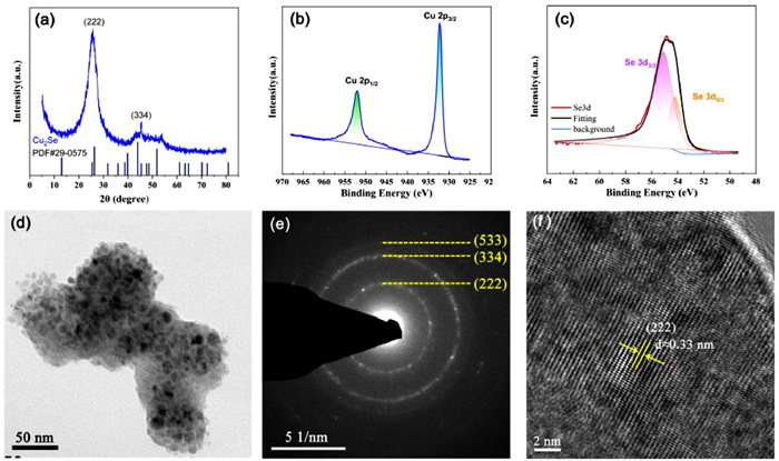
The phase, surface element valence state and crystal structure of the as-deposited Cu2Se@C thin film were revealed by XRD, XPS and TEM. The XRD pattern of the as-deposited Cu2Se@C thin film (Fig. 2a) exhibits a broad peak at 26° and a small peak at 45°, which match well with the (222) and (334) planes of Cu2Se (PDF#29–0575), respectively [33]. As exhibited in Fig. S2 (Supporting information), the XRD pattern of the well crystallized commercial Cu2Se powder can also well match the standard PDF card of Cu2Se (PDF#29–0575). The Cu 2p and Se 3d peaks are shown in survey spectrum of the Cu2Se@C thin film (Fig. S3 in Supporting information). As shown in Fig. 2b, Cu 2p1/2 at 952.60 eV and Cu 2p3/2 at 932.60 eV are the characteristic peaks of Cu+ [34,35]. Fig. 2c depicts the high-resolution XPS spectrum of Se 3d, and the splitted Se 3d3/2 peak at 55.09 eV and Se 3d5/2 peak at 54.18 eV can be assigned to Se2− [14,34,35]. What is more, the element ratio of Cu: Se counted by XPS is about 2.0. Combining the results of element valence state and element ratio, we can draw a conclusion that the phase of the as-deposited film is Cu2Se. The TEM image (Fig. 2d) again verifies that the film is constituted of numerous nanoparticles. There are three polycrystalline diffraction rings displayed in SAED (Fig. 2e), which can be indexed to (222), (334) and (533) planes of Cu2Se, respectively. Fig. 2f is the high-resolution TEM image of the as-deposited film, and the lattice fringe of 0.33 nm can be assigned to the (222) plane of Cu2Se. In conclusion, based on the results of multiple technical analyses (XRD, XPS, TEM), the component and phase of the thin film deposited by electrochemical deposition method is Cu2Se.
The formation of Cu2Se phase during electrochemical deposition process can be divided into two successive steps: First, the Cu2+ is complexed with citrate to form CuCit−. Then, the SeO32− is reduced to Se2−, and further combined with CuCit− to form Cu2Se solid. The reaction process can be described by the following equations [36]:
|
|
(1) |
|
|
(2) |
The electrochemical performance of the Cu2Se@C was tested by R2025 coin cells assembled by employing Cu2Se@C as cathode, Cu foil as anode and 0.5 mol/L CuSO4 as electrolyte. Fig. 3a shows the cyclic voltammetry (CV) curves of the commercial Cu2Se powder and the Cu2Se@C film at a scan rate of 0.05 mV/s in a voltage window of 0–0.5 V (vs. Cu2+/Cu). For Cu2Se@C electrode, three oxidation peaks are presented in oxidation process. The oxidation peak at 0.09 V is relatively small, and two larger oxidation peaks at 0.23 and 0.27 V overlap each other. During the reduction process, three reduction peaks correspond well to the three oxidation peaks, indicating the great reversibility of the Cu2Se@C electrode. Two larger reduction peaks (0.13 and 0.11 V) close together, and a tiny reduction peak is observed at a low potential of 0.07 V. The redox peaks always correspond to the phase transition during scanning, declaring that the Cu2Se@C electrode undergoes a multiphase transition in the redox process. The potential differences between the oxidation peaks and the reduction peaks of the Cu2Se@C film are less than those of the commercial Cu2Se powder due to the smaller internal resistance and the less polarization potential generated by the well-designed Cu2Se@C film.
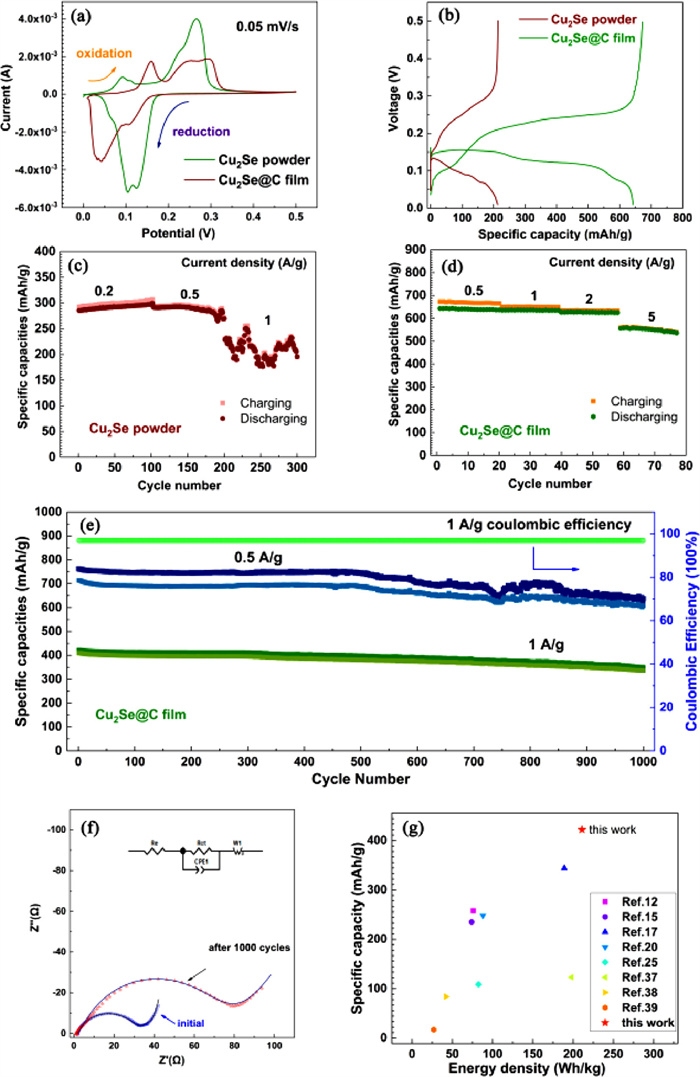
The GCD curves at 0.5 A/g in the potential range of 0–0.5 V are shown in Fig. 3b. Compared with the commercial Cu2Se powder, the Cu2Se@C film displays higher specific capacities and more stable voltage platform, which indicates that the Cu2Se@C film with the three-dimensional braided structure can effectively improve energy storage capacity. In the charge curve of the Cu2Se@C film, the short voltage platform with the scope of 0.09–0.12 V and two slope long voltage platforms (0.19–0.22 V and 0.22–0.26 V) are in great agreement with the three oxidation peaks at 0.09, 0.23 and 0.27 V, respectively. During discharging, the discharge platforms of 0.18–0.16 V, 0.15–0.12 V and 0.09–0.05 V well match the reduction peaks of 0.13, 0.11 and 0.07 V. The GCD curves again verify that the Cu2Se@C electrode undergoes a multiphase transition during charging-discharging, which will be discussed later.
To investigate the rate performance of the Cu2Se powder and the Cu2Se@C film, the assembled coin cells were tested at current densities from 0.2 A/g to 5 A/g. The discharge specific capacities of the commercial Cu2Se powder are about 297 mAh/g at 0.2 A/g and 291 mAh/g at 0.5 A/g (Fig. 3c), and the charging and discharging process becomes unstable when the current density increases to 1 A/g. As demonstrated in Fig. 3d, the Cu2Se@C electrode shows superb rate performance, and the discharge specific capacities at 0.5, 1, 2, 5 A/g are 640, 635, 627, 542 mAh/g, respectively. Fig. 3e exhibits the long cycling stability of the Cu2Se@C film at current densities of 0.5 and 1 A/g for 1000 cycles. The first charge and discharge specific capacities at 0.5 A/g are about 762 and 714 mAh/g, respectively. After 1000 cycles, the charge and discharge specific capacities can still be kept at 629 and 607 mAh/g, respectively. When tested at 1 A/g, the Cu2Se@C electrode shows the first charge and discharge specific capacities of 422 and 409 mAh/g, respectively. After 1000 long cycles, the charge and discharge specific capacities maintain at 349 and 336 mAh/g, respectively. During the long 1000 cycles, the capacity retention rate is 82.7%, which means the average capacity decay rate is as low as 0.017%. What is more, the Coulombic efficiency of the Cu2Se@C electrode at 1 A/g remains unchanged at about 97% from the 1st cycle to the 1000th cycle. The excellent cycling stability is mainly attributed to the three-dimensional braided structure of the Cu2Se@C thin film and the good connection between active material and carbon fibers.
The Nyquist plots of the Cu2Se powder and the Cu2Se@C electrode are illustrated in Fig. S4 (Suporting information) and Fig. 3f, which are composed of two parts: A high-frequency semicircle and a low-frequency diagonal line. The inset is the fitted equivalent circuit. Re represents the internal resistance, Rct means the charge transfer resistance, W1 is the warburg resistance, which is associated with the ion diffusion in electrode. The Rct of the Cu2Se powder is about 380 Ω. It is obvious that the Rct of the Cu2Se@C electrode before cycling is relatively small (about 29.39 Ω), which benefits from the one-piece binder-free design. The well-designed structure and the immediate contact between active material and current collector will accelerate the fast movement of the charge. After 1000 cycles, the Rct increases slightly to 61.16 Ω, which may be due to the volume expansion during the charge-discharge. The impact associated with the volume expansion includes inadequate contact between active material (Cu2Se layer) and current collector (carbon clothes), which may increase the interface resistance and further bring about the capacity fading.
Fig. 3g is the comparison of specific capacities and energy densities of the previously reported Se-based electrode materials at 1 A/g with those of the Cu2Se@C electrode in this work [12,15,17,20,25,37–39]. It is obvious that the Cu2Se@C electrode in this work shows higher specific capacities and energy densities at the same current density, demonstrating that the Cu2Se@C electrode with admirable electrochemical performance is of great significance for the development of new electrode material systems.
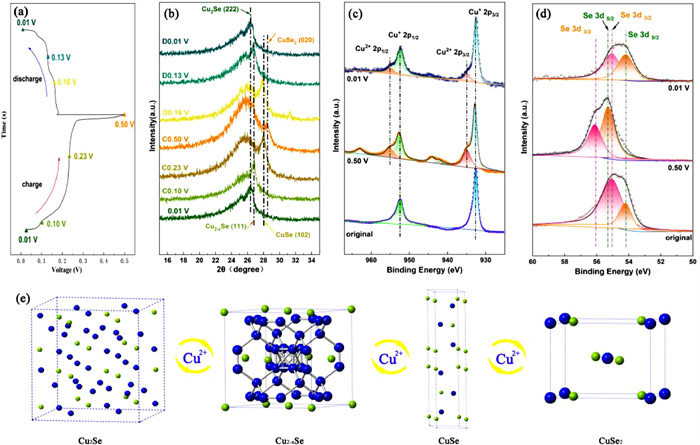
For the purpose of revealing the electrochemical behavior and energy storage mechanism of the Cu2Se@C electrode, ex situ XRD and XPS were employed to explain and give evidence of the phase transition process and the variations of valence state of the elements during charge and discharge process. Fig. 4a is the GCD curve of the Cu2Se@C electrode at 0.1 A/g, in which we choose some research points (charging to 0.10, 0.23, 0.50 V and discharging to 0.16, 0.13, 0.01 V) for ex situ XRD analyses. The ex situ XRD analyses of the Cu2Se@C electrode at different charge-discharge states are illustrated in Fig. 4b. When charging to 0.10 V, the main peak shifts to the right, which can well match the (111) plane of Cu2-xSe (PDF#06–0680, space group of F43m, a = b = c = 0.5739 nm, α = β = γ = 90°) with an interplanar spacing of 0.333 nm [40]. With further oxidation to 0.23 V, the phase of the cathode changes to CuSe (PDF#34–0171, space group of P63/mmc, a = b = 0.3939 nm, c = 1.725 nm, α = β = 90°, γ = 120°) and the diffraction peak can correspond to the (102) plane with an interplanar spacing of 0.317 nm. [34] At the end of the charging process (charging to 0.5 V), the diffraction peak moves to the far right and can be assigned to the (020) plane of CuSe2 (PDF#18–0453, space group of Pnnm, a = 0.509 nm, b = 0.628 nm, c = 0.38 nm, α = β = γ = 90°) with an interplanar spacing of 0.313 nm [41]. During the reduction process, the characteristic diffraction peaks gradually shift back to the left and the phases of the Cu2Se@C electrode can be identified as CuSe, Cu2-xSe and Cu2Se when discharging to 0.16, 0.13 and 0.01 V, respectively. Notably, when discharging to 0.01 V, the phase of active material can return back to Cu2Se, which is the crucial evidence for the admirable cyclic reversibility of the Cu2Se@C electrode. Based on the phase components and phase evolution of the Cu2Se@C electrode during the charging process, the conversion process can be summarized as: Cu2Se ↔ Cu2-xSe ↔ CuSe ↔ CuSe2, and the corresponding crystal structure transition is illustrated in Fig. 4e. As mentioned before, the redox peaks in the CV curve and the voltage platform in the GCD curve are caused by the phase transition between Cu2Se, Cu2-xSe, CuSe and CuSe2. Additionally, the cathodic reaction equation during charging and discharging can be written as:
|
|
(3) |
Based on this equation, the average 1 mol Cu2Se can store 1.5 mol Cu2+ and transfer 3 mol e−, and it is easy to calculate the theoretical specific capacity of Cu2Se (780.39 mAh/g), which is far beyond other aqueous battery cathode materials, such as MnO2 (308 mAh/g) [7] and vanadium-based oxides (about 300 mAh/g) [42] in zinc ion batteries.
The comparison of the surface valence states of Cu and Se elements of the Cu2Se@C electrode at different states (the original state, charging to 0.50 V and discharging to 0.01 V) is verified by XPS. As shown in Fig. 4c, only two characteristic peaks of Cu+ present at 952.60 eV (Cu 2p1/2) and 932.60 eV (Cu 2p3/2) at the original state. When charging to 0.50 V, despite the remain of the characteristic peaks of incompletely oxidized Cu+, the characteristic peaks of Cu2+ (Cu 2p1/2 at 955.00 eV, Cu 2p3/2 at 934.85 eV) and corresponding satellite peaks appear distinctly [43,44]. The transformation from Cu+ to Cu2+ is due to the oxidation reaction resulting from the de-intercalation of Cu2+ from the Cu2Se@C electrode during the charging process. When discharging to 0.01 V, the high-resolution XPS spectrum of Cu 2p demonstrates the weakened characteristic peaks of Cu2+ and the enhanced characteristic peaks of Cu+, indicating the reduction of Cu2+ to Cu+ during the discharging process. As presented in Fig. 4d, at the original state, the Se 3d splits into Se 3d3/2 peak at 55.09 eV and Se 3d5/2 peak at 54.18 eV, which can be assigned to Se2−. When fully charging to 0.50 V, the Se 3d of the Cu2Se@C electrode with Se 3d3/2 at 56.12 eV and Se 3d5/2 at 55.29 eV shift to higher binding energy region which can be indexed as the existence of Se22− specie in the CuSe2 [44,45]. When discharging to 0.01 V, the peaks of Se 3d move back to the right and the Se22− turns back to Se2−. In conclusion, combining with the analyses of XRD in Fig. 4b, the species of the active material in fully oxidated electrode are Cu2+ and Se22− in CuSe2 phase, the Cu2+ will convert to Cu+ and Se22− will turn back to Se2− to form Cu2Se during the discharging process.
To further explore the kinetic characteristic of the Cu2Se@C electrode, the ion diffusion coefficient in the Cu2Se@C electrode was measured by CV, GITT and EIS tests. Fig. 5a displays the CV curves of the Cu2Se@C electrode at different scan rates in a range of 0.05–0.20 mV/s. With the increase of the scan rates, the areas and peak currents of the CV curves increase due to the polarization. The energy storage mechanism of the electrode based on the control steps in the charge-discharge process can be divided into two categories: the diffusion control model or surface adsorption control model. The control model can be distinguished by the relationships between peak current (I) and scan rate (v):
|
|
(4) |
where a and b are the constant parameters, b = 0.5 means the diffusion control model, while b = 1 represents the surface adsorption control model. According to the fitted line plot of I(mA) versus v−1/2 (mV1/2 s−1/2) of the Cu2Se@C electrode (Fig. 5b), the linear relationship between I(mA) and v−1/2 (mV1/2 s−1/2) fits well, indicating that the Cu2Se@C electrode belongs to the diffusion control model. The diffusion coefficient of Cu2+ in the Cu2Se@C electrode can be calculated by Randles-Sevcik equation:
|
|
(5) |
where I is the peak current in CV curve, n means the number of transfer charges, A corresponds to the electrode area, C represents the Cu2+ concentration, D is the ion diffusion coefficient, and v is the scan rate [46]. By comparing the calculated Cu2+ diffusion coefficient (DCu2+) of the redox peaks in the CV curves shown in Table S1 (Supporting information), the DCu2+ (about 10−10–10−9) in the oxidation peaks is slightly inferior to the DCu2+ (about 10−9) in the reduction peaks. GITT test was also utilized to investigate the dynamic electrochemical behavior, and the ion diffusion coefficient can be calculated by:
|
|
(6) |
where τ is relaxation time, nm, Vm and S are the mole number, molar volume and area of the active material, respectively. △Es and △Et are the voltage changes resulting from the impulse and constant current charge and discharge, respectively [47].
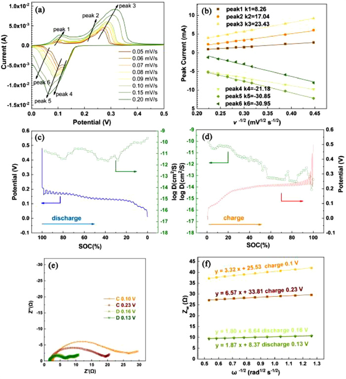
Figs. 5c and d demonstrate the discharge/charge process and the corresponding ion diffusion coefficients. It is obvious that the Cu2+ diffusion calculated by GITT in the discharging process (DGITT-D = 10−11–10−9) is more efficient than that in the charging process (DGITT-C = 10−14–10−10), indicating the insertion of Cu2+ in the Cu2Se@C electrode is easier than the de-intercalation. What is more, the ion diffusion coefficient of the Cu2Se@C electrode at different charge and discharge states is not exactly the same.
In order to further investigate the kinetic characteristic of the Cu2Se@C electrode at different states, the electrochemical impedance spectra were conducted when charging to 0.1, 0.23 V (C 0.1, C 0.23 V) and discharging to 0.16, 0.13 V (D 0.16, D 0.13 V), respectively (Fig. 5e). The charge transfer resistance (Rct) shown in the high-frequency semicircle at D 0.16 V (5.26 Ω) and D 0.13 V (4.96 Ω) are significantly lower than those of C 0.1 V (20.05 Ω) and C 0.23 V (16.50 Ω). Additionally, the warburg resistance illustrated in the low-frequency region can be employed to calculate the ion diffusion coefficient by using the following equations:
|
|
(7) |
|
|
(8) |
where the basic physical parameters R, F are gas constant and Faraday constant, respectively. And T, A, n and C are the parameters related to the electrochemical system: the absolute temperature (K), the surface area of the electrode (cm2), the number of electrons involved in electrochemical reaction and the concentration of Cu2+, respectively [48]. As illustrated in Fig. 5f, σw can be obtained by fitting the line plot of Zw versus w1/2. The values of DCu2+ at C 0.1, C 0.23, D 0.16 and D 0.13 V are 8.04 × 10⁻¹⁶, 2.05 × 10⁻¹⁶, 2.74 × 10⁻¹⁵, 2.54 × 10⁻¹⁵ cm2/s, respectively. The larger values of DCu2+ at D0.16 and D0.13 V again verify that the insertion of Cu2+ in the Cu2Se@C electrode is easier than the de-intercalation. Combining the ex situ XRD analyses discussed in Fig. 4b, during the discharging process, the phase of the Cu2Se@C electrode is orderly converted from CuSe2 to CuSe, Cu2-x Se and Cu2Se, and the corresponding interplanar spacings increase gradually (Table S2 in Supporting information), which may lead to the easier insertion of Cu2+ in the Cu2Se@C electrode than the de-intercalation.
In conclusion, the Cu2Se@C thin film electrode with three-dimensional structure was fabricated by a simple and easy electrochemical deposition method, and further utilized as cathode material for Cu2+ storage. Featuring the advantages of the one-piece designed structure, high ionic conductivity and large interplanar spacing of the Cu2Se@C thin film, the as-assembled "Cu|0.5 mol/L CuSO4| Cu2Se@C" coin cell demonstrates high specific capacity of 640 mAh/g at 0.5 A/g, superb rate capability of 542 mAh/g at 5 A/g, and high electrochemical stability with 82.7% capacity retention at 1 A/g with a remarkable durability up to 1000 cycles. The Cu2Se@C electrode undergoes a sequential conversion of Cu2Se ↔ Cu2-xSe ↔ CuSe ↔ CuSe2, and the electrode reactions can be summarized as follows: cathode: CuSe2 + 3Cu2+ + 6e− ↔ 2Cu2Se; anode: 3Cu ↔ 3Cu2+ + 6e−; battery: CuSe2 + 3Cu ↔ 2Cu2Se. The kinetic characteristic of the Cu2Se@C electrode during charge/discharge process is investigated by CV, GITT, and EIS and the results reveal that the Cu2+ diffuses faster in the discharging process than the charging process. This work puts forward a facile and reliable strategy to fabricate flexible thin film electrode and opens a door for new multivalent charge carrier (Cu2+) battery, which is a promising candidate for high performance, flexible energy storage systems.
The authors declare that they have no known competing financial interests or personal relationships that could have appeared to influence the work reported in this paper.
This work is partly supported by the National Natural Science Foundation of China (No. 51972108), Distinguished Young Scientists of Hunan Province (No. 2022JJ10024), Natural Science Foundation of Hunan Province (No. 2021JJ30216), and Key Projects of Hunan Provincial Education Department (No. 22A0412).
Supplementary material associated with this article can be found, in the online version, at doi:
M. Armand, J.M. Tarascon, Nature 451 (2008) 652–657. doi: 10.1038/451652a
J.B. Goodenough, Y. Kim, Chem. Mater. 22 (2010) 587–603. doi: 10.1021/cm901452z
J.C. Stallard, L. Wheatcroft, S.G. Booth, et al., Joule 6 (2022) 984–1007. doi: 10.1016/j.joule.2022.04.001
X. Feng, D. Ren, X. He, et al., Joule 4 (2020) 743–770. doi: 10.1016/j.joule.2020.02.010
Y. Chen, Y. Kang, Y. Zhao, et al., J. Energy Chem. 59 (2021) 83–99. doi: 10.3390/membranes11020083
Y. Liang, Y. Yao, Nat. Rev. Mater. 8 (2023) 109–122.
H. Tang, W. Chen, N. Li, et al., Energy Storage. Mater. 48 (2022) 335–343. doi: 10.1016/j.ensm.2022.03.042
J. Yao, C. Liu, J. Li, et al., Rare Met. 42 (2023) 2307–2323. doi: 10.1007/s12598-023-02265-5
H. Tang, J. Yao, Y. Zhu, Adv. Energy Mater. 11 (2021) 2003994. doi: 10.1002/aenm.202003994
Y. Liu, X. Wu, Chin. Chem. Lett. 33 (2022) 1236–1244. doi: 10.1016/j.cclet.2021.08.081
K. Liang, S. Huang, H. Zhao, et al., Adv. Mater. Interfaces 9 (2022) 220564.
Y. Liu, M. Li, G. Wang, et al., Energy Environ. Mater. 4 (2021) 465–473. doi: 10.1002/eem2.12130
X. Wang, J. Zhao, Y. Chen, et al., J. Colloid Interface Sci. 628 (2022) 1041–1048. doi: 10.1016/j.jcis.2022.08.138
Q. Luo, J. Wen, G. Liu, et al., J. Power Sources 545 (2022) 231917. doi: 10.1016/j.jpowsour.2022.231917
X. Du, J. Li, K. Tong, et al., J. Alloys Compd. 899 (2022) 163359. doi: 10.1016/j.jallcom.2021.163359
Z. Lu, Z. Hu, L. Xiao, et al., Chem. Eng. J. 450 (2022) 138347. doi: 10.1016/j.cej.2022.138347
M. Ahmad, I. Hussain, T. Nawaz, et al., J. Power Sources 534 (2022) 231414. doi: 10.1016/j.jpowsour.2022.231414
H. Wanga, Y. Zhong, J. Ning, et al., Chin. Chem. Lett. 32 (2021) 3733–3752. doi: 10.1016/j.cclet.2021.04.025
M. Rashad, S.D.A. Zaidi, M. Asif, J. Magnes. Alloy. 8 (2020) 980–988. doi: 10.1016/j.jma.2020.05.016
Y. Deng, Y. Chen, X. Zhang, et al., J. Alloys Compd. 892 (2021) 162159.
X. Wang, M. Zhang, H. Mei, et al., Ceram. Int. 47 (2021) 24699–24706. doi: 10.1016/j.ceramint.2021.05.192
J. Zhang, X. Zhang, C. Xu, et al., Adv. Energy Mater. 12 (2022) 2103998. doi: 10.1002/aenm.202103998
Y. Xiao, X. Zhao, X. Wang, et al., Adv. Energy Mater. 10 (2020) 2000666. doi: 10.1002/aenm.202000666
Y. Yang, J. Xiao, J. Cai, et al., Adv. Funct. Mater. 31 (2020) 2005092.
Y. Zhu, H. Tang, X. Yun, et al., J. Alloys Compd. 866 (2021) 158972. doi: 10.1016/j.jallcom.2021.158972
Q. Gao, P. Li, S. Ding, et al., Ionics 26 (2020) 5525–5533. doi: 10.1007/s11581-020-03686-3
H. Shi, G. Wen, Y. Nie, et al., Nanoscale 12 (2020) 5261–5285. doi: 10.1039/c9nr09785f
H. Li, J. Gong, J. Li, et al., Chin. Chem. Lett. 31 (2020) 2275–2279. doi: 10.1016/j.cclet.2020.03.010
W. Chen, H. Zhang, Y. Zhu, et al., J. Colloid Interface Sci. 611 (2022) 183–192. doi: 10.1016/j.jcis.2021.12.074
S. Yang, Y. Cui, G. Yang, et al., J. Power Sources 554 (2023) 232347. doi: 10.1016/j.jpowsour.2022.232347
H. Sun, J. Zhu, D. Baumann, et al., Nature Rev. Mater. 4 (2019) 45–60.
K. Liang, H. Zhao, J. Li, et al., Small 19 (2023) 2207562. doi: 10.1002/smll.202207562
S. Ballikaya, H. Chi, J.R. Salvador, et al., J. Mater. Chem. A 1 (2013) 12478–12484. doi: 10.1039/c3ta12508d
X. Li, W. Lv, G. Wu, et al., Chem. Eng. J. 426 (2021) 131899. doi: 10.1016/j.cej.2021.131899
X. Chen, M. Li, S. Wang, et al., Adv. Sci. 9 (2022) 2104.
W. Tan, H. He, Y. Gao, et al., J. Colloid Interface Sci. 600 (2021) 492–502. doi: 10.1016/j.jcis.2021.05.002
L. Hou, X. Sun, L. Guo, et al., Energy Technol 8 (2020) 1901319. doi: 10.1002/ente.201901319
Y. Zhu, X. Yun, J. Li, et al., J. Electrochem. Soc. 165 (2018) A3723–A3731. doi: 10.1149/2.0371816jes
L. Hou, Y. Shi, C. Wu, et al., Adv. Funct. Mater. 28 (2018) 1705921. doi: 10.1002/adfm.201705921
H. Liang, Z. Liang, Z. Li, et al., Ceram. Int. 48 (2022) 248–255. doi: 10.1016/j.ceramint.2021.09.099
L. Zhao, N. Lin, Z. Han, et al., Adv. Electron. Mater. 5 (2019) 1900485. doi: 10.1002/aelm.201900485
Y. Mei, Y. Liu, W. Xu, et al., Chem. Eng. J. 452 (2023) 139574. doi: 10.1016/j.cej.2022.139574
A. Olvera, P. Sahoo, S. Tarczynski, et al., Chem. Mater. 27 (2015) 7179–7186. doi: 10.1021/acs.chemmater.5b03630
A.V. Tran, T.T. Nguyen, H.J. Lee, et al., Appl. Catal. A: Gen. 587 (2019) 117245. doi: 10.1016/j.apcata.2019.117245
T. Liu, Z. Jin, J. Li, et al., Cryst. Eng. Comm. 15 (2013) 8903–8906. doi: 10.1039/c3ce41500g
Y. Zhang, P. Chen, Q. Wang, et al., Adv. Energy Mater. 31 (2021) 2101712.
N. Zhang, M. Jia, Y. Dong, et al., Adv. Funct. Mater. 29 (2019) 1807331. doi: 10.1002/adfm.201807331
J. Huang, Z. Wang, M. Hou, et al., Nat. Commun. 9 (2018) 2906. doi: 10.1038/s41467-018-04949-4

Figure 1 (a) Schematic illustration of the electrodeposition process. SEM surface observation of (b) carbon clothes and (c-e) Cu2Se@C thin film. (f) The morphology of cross-section and (g) EDS elemental mapping of Cu2Se@C.

Figure 2 (a) XRD pattern of Cu2Se@C. XPS spectra of (b) Cu 2p and (c) Se 3d. (d) TEM, (e) SAED and (f) HRTEM images of Cu2Se@C.

Figure 3 The electrochemical performance of the Cu2Se powder and the Cu2Se@C film. (a) CV curve. (b) GCD curve. The rate performance of (c) Cu2Se powder and (d) Cu2Se@C film. (e) The long cycling performance and (f) EIS of the Cu2Se@C film. (g) The comparison of specific capacities and energy densities of Se-based electrode materials in literatures with this work (the Cu2Se@C film).

Figure 4 The electrochemical conversion process of the Cu2Se@C electrode. (a) GCD curve at 0.1 A/g. (b) The ex situ XRD analyses at different charging states (0.1, 0.23, 0.5 V) and discharging states (0.16, 0.13, 0.01 V). The ex situ XPS spectra of (c) Cu 2p and (d) Se 3d at different potentials. (e) Schematic illustration of the crystal structure transition of Cu2Se upon Cu2+ insertion and de-intercalation.

Figure 5 The kinetic characteristic of the Cu2Se@C cathode. (a) CV curves at different scan rates and (b) the corresponding linear fitting of the log(I) versus log(v−1/2). GITT profiles and corresponding ion diffusion coefficient in (c) discharge and (d) charge process. (e) EIS at different charge and discharge states and (f) the corresponding linear fitting of ZW versus ω−1/2.

 扫一扫看文章

扫一扫关注我们
 DownLoad:
 下载:
下载: