Citation:
Yao Ni, Lu Liu, Jiulong Feng, Lu Yang, Wentao Xu. Flexible organic artificial synapse with ultrashort-term plasticity for tunable time-frequency signal processing[J]. Chinese Chemical Letters,
2023, 34(12): 108419.
doi:
10.1016/j.cclet.2023.108419
Flexible organic artificial synapse with ultrashort-term plasticity for tunable time-frequency signal processing
English
Flexible organic artificial synapse with ultrashort-term plasticity for tunable time-frequency signal processing
Institute of Photoelectronic Thin Film Devices and Technology, Key Laboratory of Photoelectronic Thin Film Devices and Technology of Tianjin, College of Electronic Information and Optical Engineering, Engineering Research Center of Thin Film Photoelectronic Technology of Ministry of Education, Smart Sensing Interdisciplinary Science Center, Nankai University, Tianjin 300350, China
b.
Shenzhen Research Institute of Nankai University, Shenzhen 518000, China
* Corresponding author. E-mail address: wentao@nankai.edu.cn (W. Xu). 1 These authors contributed equally to this work.
Received Date:
01 February 2023 Accepted Date:
02 April 2023 Revised Date:
31 March 2023 Available Online:
15 December 2023
Abstract:
A flexible organic artificial synapse (OAS) for tunable time-frequency signal processing was fabricated using a tri-blend film that had been fabricated using a one-step solution method. When combined with a chitosan film, this OAS can achieve an ultrashort-term retention time of only 49 ms for instant electrical-computing applications; this is the shortest retention time yet achieved by a two-terminal artificial synapse. An array of these flexible OASs can withstand a high bending strain of 5% for 104 cycles; this deformation endurance is a new record. The OAS was also sensitive to the number and frequency of electrical inputs; a tunable cut-off frequency enables dynamic filtering for use in image detail enhancement. This work provides a new resource for development of future neuromorphic computing devices
Neuromorphic computing emulates the organization of a brain, in which memory and processing are performed using the same units; this architecture can easily process unstructured and complexed problems [1-4]. This ability can overcome the limitation of traditional digital computers, which are constructed using ‘von Neumann’ architecture, which physically separates memory modules from processors, so information must be shuttled between the two components; consequently, these computers cannot efficiently process unstructured information [5].
Synapses are the basic unit of brain cognition. They support a variety of complex perceptual and cognitive processes. Artificial synapses (ASs) have been developed for use in construction of an architecture that has brain-like ability [6,7]. However, these AS devices had an insufficient short-term response characteristic and a long reset time, which can cause aliasing or missing when processing real-time frequency signals [6-8]. Furthermore, most reported ASs have been constructed from inorganic brittle materials that were incompatible with flexible functionalities [9]. To overcome this problem, use of a flexible blend organic interface that operates by dynamic charge/ion mechanism has been proposed.
In this work, we designed an organic artificial synapse (OAS) that is fabricated using poly(3-hexylthiophene) (P3HT), 2,7-dioctylbenzothieno[3,2-b]benzothiophene (C8BTBT), and poly(methyl methacrylate) (PMMA) tri-blend film for tunable time-frequency signal processing. When combined with a chitosan film, OAS can form domains of short-term order in the channel under negative voltage spikes; this change improves hole-carrier transport to trigger a short-term excitatory postsynaptic response. The OAS had an ultrashort-term plasticity with charge carrier retention time of only 49 ms, which is the best het achieved for a two-terminal artificial synapse. An OAS array endured 104 bending cycles of a 5% strain, a new record for mechanical flexibility. The OAS array had the time-frequency property of being sensitive to the number of presynaptic spikes. In a demonstration of dynamic image processing, this property enabled high-pass filtering with a tunable cut-off frequency. This study provides a useful resource that can have applications in wearable biomedical electronics and neuromorphic computing.
A mixed organic solution was obtained by P3HT, C8BTBT and PMMA with a proportion of 2 wt%:2 wt%:0.4 wt% dissolved in chlorobenzene at room temperature. 2 wt% chitosan and 2 wt% acetic acid were dissolved in 96 wt% deionized water at room temperature. Then, the chitosan solution was dip-coated onto a mold and dried in air ambient to form a homogeneous chitosan electrolyte film.
To fabricate the OAS (Fig. 1a), low-resistivity p-type silicon (Si) wafers were used as the bottom electrodes. Then, the mixed organic solution of P3HT:C8BTBT:PMMA was spin-coated onto the Si wafers at 4000 rpm for 40 s. The prepared samples were vapor-annealed in a sealed environment with 120 ℃ chlorobenzene steam for 1 h; the blend film can become phase-separated during this process. The samples were annealed again in a nitrogen atmosphere at 60 ℃. Chitosan films as the ion-gel layer were transferred onto the samples. Finally, top electrodes were thermally deposited through a shadow mask onto the chitosan/blend organic layers.
Figure 1
Figure 1.
(a) Schematic illustrations of an OAS device. (b) Cross-sectional SEM (left) and EDS (right) images of the tri-blend organic layer on a p-type Si substrate. (c) AFM images of P3HT:PMMA blend film (left), C8BTBT:PMMA blend film (middle) and tri-blend film (right). (d) Corresponding CPD of the tri-blend organic layer on a p-type Si substrate using the KPFM mode after top bias of 0 V (initial state), −4 V and 0 V (withdraw the top bias) on the AFM tip. (e) C-V curve of chitosan film. (f) Schematic diagram of device structure, ion migration and electric field distribution under bias.
We acquired a scanning electron microscopy (SEM) image of the cross section with an FEI-Apreo field emission microscope. The film topography was measured in tapping mode using a Bruker dimension icon atomic force microscope (AFM); contact potential difference distribution (CPD) values were obtained with the situ Kelvin probe force microscopy (KPFM) mode. The capacitance-voltage C-V properties of the chitosan film were measured by using an electrochemical workstation (CHI760E). All electrical characteristics and synaptic functions of the OAS device were carried out using a Keithley 4200A semiconductor parameter analyzer with a preamplifier (4200-PA) in a nitrogen-filled glovebox.
To simulate a high-pass filter, a target image was first converted from spatial domain to frequency domain, then the matrix in the frequency domain was rearranged by moving the zero-frequency component to the center. A m × n high-pass filter template was established by exploiting the filtering behavior of the OAS high-pass filter: The Euclidean distance between the center (0.5m, 0.5n) and a specific point (i, j) was set as the cut-off frequency fc. The filtering was implemented by utilizing a matrix G = H(i, j)N(i, j). G was decentralized and transformed to a matrix in the spatial domain to obtain the filtered result.
A schematic of the OAS with a vertical channel is demonstrated (Fig. 1a). A cross-sectional SEM image of the tri-blend organic layer on a p-type Si substrate was obtained to enable the study of the phase separation (Fig. 1b). The bright area in the section represented PMMA with a poor conductivity (Fig. 1b, left). Energy dispersive spectrometry (EDS) analysis identified sulfur mainly gathering in the top layer (Fig. 1b, right). This result confirms that the vertically stratified structure consists of a sulfur-containing P3HT:C8BTBT upper layer and a non-sulfur PMMA lower layer. Here, the PMMA layer is thin enough for charge carriers to tunnel away along the channel directions when an electric field is applied. Pure P3HT and pure C8BTBT formed order domains but with distinct morphology (Fig. 1c, left and middle): C8BTBT domains were large with deep gaps, whereas P3HT domains were small. In the tri-blend layer, the P3HT:C8BTBT upper layer cannot form a relatively flat and ordered domain interface (Fig. 1c, right), which provides a precondition to shorten the retention time of charge carriers in the channel [10,11].
For proving the charge-retention capability in relation to the film morphology, the CPD values of P3HT:C8BTBT:PMMA blend film prepared based on a Si architecture were investigated with various bias on the top terminal (Fig. 1d). In the initial state without bias, the CPD was 323.8 mV (Fig. 1d, left). Under a top bias of −4 V, a lower CPD of 298.2 mV confirmed the hole-trapping state in the tri-blend film (Fig. 1d, middle). Once withdrawing the top bias, the CPD quickly recovered to 323.5 mV, which was only 0.3 mV from the initial value (Fig. 1d, right); both P3HT:PMMA and C8BTBT:PMMA blend films exhibited a high CPD difference between before and after the top bias, reaching 3.5 mV and 8.6 mV, respectively (Fig. S1 in Supporting information). This result further verified the obvious advantages of the tri-blend film in hole carriers’ rapid de-trapping process.
The chitosan film on the blend organic layer can be regarded as a capacitor (Fig. 1e): The positively charged protons are driven to move toward the blend layer under a positive bias, but to the top electrode under a negative bias [12]. Thus, once a negative bias was applied to the chitosan film, the positive charges on the blend organic channel’s thiophene rings and the negative charges on the anions served to bind the host and dopant subsystems to form domains of short-term order, in which the ions were intercalated between the planar conjugated backbones of the polymer channel; this structure increases the instantaneous migration efficiency of the charge carriers (Fig. 1f) [13].
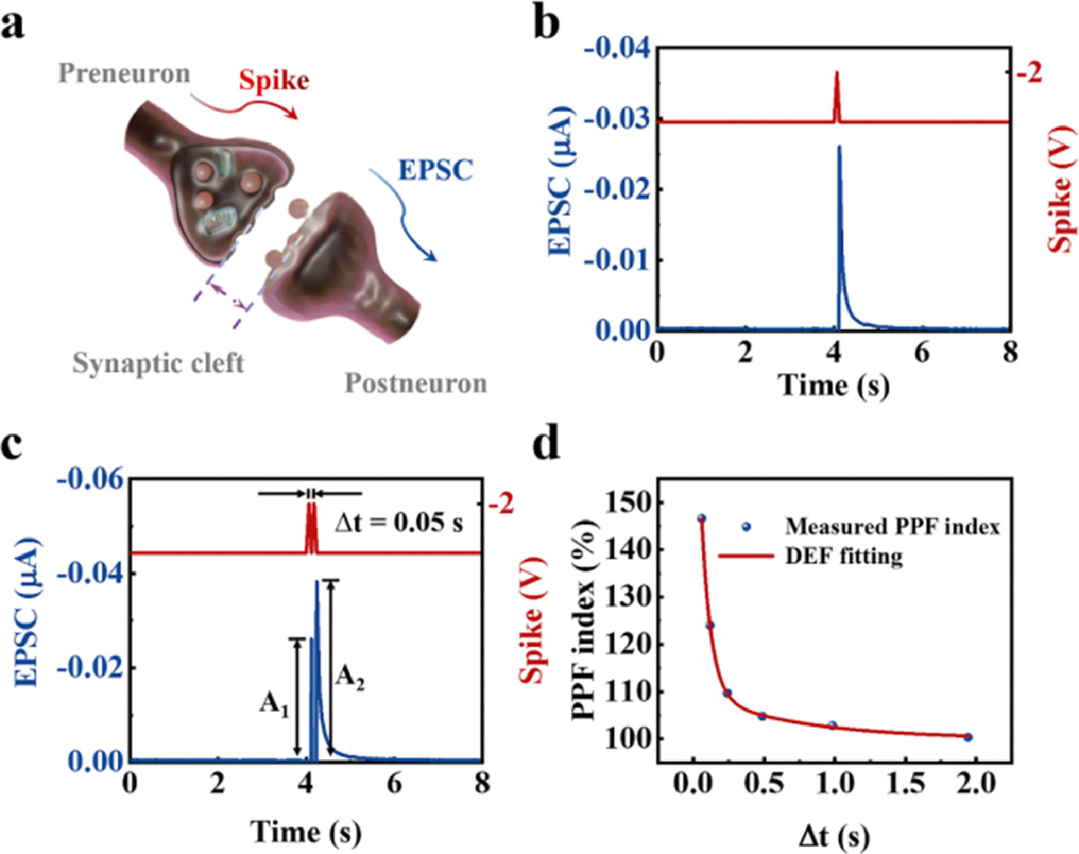
Stimulation of a biological neuron causes propagation of a depolarization along its axon; when the pulse reaches the synaptic cleft between the stimulated (preneuron) and the next (postneuron) the depolarization causes secretion of neurotransmitters, which diffuse across the cleft and stimulate or inhibit responses in the postneuron (Fig. 2a). The activity of the chitosan/blend organic layers is analogous to the transmission of neurotransmitters in the synaptic cleft: when negative electrical spikes are applied, the anions migrate in the junction, and can regulate its ion-storage capacity to adjust synaptic connection strength, and thus trigger an excitatory postsynaptic current (EPSC). A negative spike of −2 V was applied to the top electrode for 0.05 s, and a primordial potential was maintained at −0.1 V (Fig. 2b). The EPSC gradually decayed to the initial state after a sharp increase in magnitude to a peak of −26 nA. In biology, neural facilitation occurs at neuromuscular junctions. A small fraction of ions responds to the first action potential, whereas most of them enter the terminal in response to the second action potential, so the second response is larger than the first. This paired-pulse facilitation (PPF) response was observed in the OAS devices and is reversible. When two consecutive spikes with a pulse intervals Δt were applied, the second EPSC (A2) was higher than the first EPSC (A1) (Fig. 2c and Fig. S2 in Supporting information). We calculated PPF index as A2/A1 × 100% (Fig. 2d). As the interval increased from 0.05 s to 1.94 s, the index decreased exponentially from 146.6% to 100.3%. The decay of the PPF index with the increase of Δt fits a double exponential fitting (DEF) equation with a rapid decay and a slow decay (Eq. 1) [14]:
(1)
Figure 2
Figure 2.
(a) Schematic illustrations of a biological synapse. (b) EPSC triggered with a presynaptic spike (amplitude = −2 V, duration = 0.05 s) and a primordial potential of −0.1 V is applied. (c) The EPSCs measured with a pair of presynaptic spikes (amplitude = −2 V, duration = 0.05 s, and ∆t = 0.05 s). (d) PPF index plotted as a function of ∆t.
where Ci and τi represent the initial facilitation magnitudes and characteristic relaxation time of rapid (i = 1) and slow (i = 2) phases, respectively. Fitted results gave τ1 = 67 ms and τ2 = 709 ms; both were comparable to those of biological synapses.
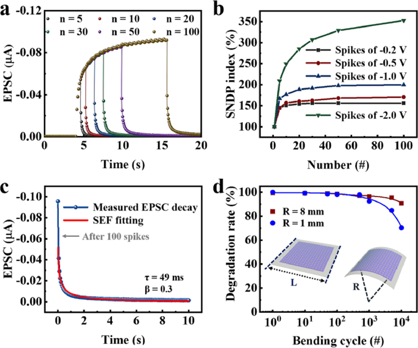
Repetitive stimuli can cause additional release of neurotransmitters and adjust the synaptic connection between neurons; this response is called spike-number dependent plasticity (SNDP) [15]. When stimulated with a series of spikes with different numbers, the OAS emulated SNDP (Fig. 3a). As the number n of spikes increased, the EPSC increased progressively at the same stimulus voltage of −2 V. This result indicates that the increase in n induces additional ions to migrate from balanced positions in the chitosan, and thus leads to an increase in channel conductivity. SNDP indexes (An/A1 × 100%) triggered by different stimulus voltages were also recorded (Fig. 3b and Fig. S3 in Supporting information); as the magnitude of the stimulus intensity was increased by a factor of 10 from −0.2 V to −2 V, the SNDP index increased by a factor of ~5; the slope is < 1, which is ascribed to a decreased diffusion of ions because they were being driven into an increasing concentration gradient. To quantify the short-term plasticity (STP) in real-time signal processing, the EPSC-retention curves were fitted using a simple first-order stretched exponential function (SEF) (Eq. 2) [1]:
(2)
where t0 is the time that the pulse finishes, I0 is the initial EPSC when the presynaptic spike finishes, I∞ is the final EPSC in an equilibrium state, 0 ≤ β ≤ 1 is a stretch index, and τ is the retention time. In our OAS devices, τ was 49 ms under 100 spikes (Fig. 3c); this is the shortest retention time among current two-terminal artificial synapses (Table S1 in Supporting information) [16-21]. Two synaptic devices with the architectures of P3HT:PMMA and C8BTBT:PMMA blend layers were prepared as the control group, the τ measured as 531 ms and 612 ms were far higher than that of the as-proposed OAS (Fig. S4 in Supporting information). This phenomenon is attributed to the mismatch spatial domains of the P3HT:C8BTBT blend film, which shortens the transmission life of hole carriers [10,11].
Figure 3
Figure 3.
(a) EPSCs triggered by different numbers of presynaptic spikes (amplitude = −2 V, duration = 0.05 s). (b) SNDP index according to the number of presynaptic spikes, with different presynaptic spike amplitudes. (c) EPSC-retention curve of OAS after 100 presynaptic spikes (amplitude = −2 V, duration = 0.05 s). (d) EPSC-degradation rates according to the number of bending cycles to curvature radii of 8 mm and 1 mm, respectively.
For a flexible integration, the blend organic film was deposited on a flexible ITO/PEN substrate, then covered with chitosan; a 16 × 16 array of top electrodes was deposited by evaporation. The resulting OAS array had a side length of 2.5 cm (Fig. 3d). We applied 100 presynaptic spikes each time on the array after it bent various curvature radii (R = 8 and 1 mm). The tensile strains S were calculated as 0.625% and 5% with the formula S = T/2R, where T is the thickness of the device (0.1 mm). The current peak weakened negligibly after the array conducted bent once at 0.625% strain, and retained 90.6% of the initial current after 104 bending cycles. Additionally, OAS can also withstand a 5% strain for 104 cycles, and the current peak retained above 70% of the initial value. This is the best electrical stability at bending tests among current flexible two-terminal artificial synapses (Table S2 in Supporting information) [22-36].
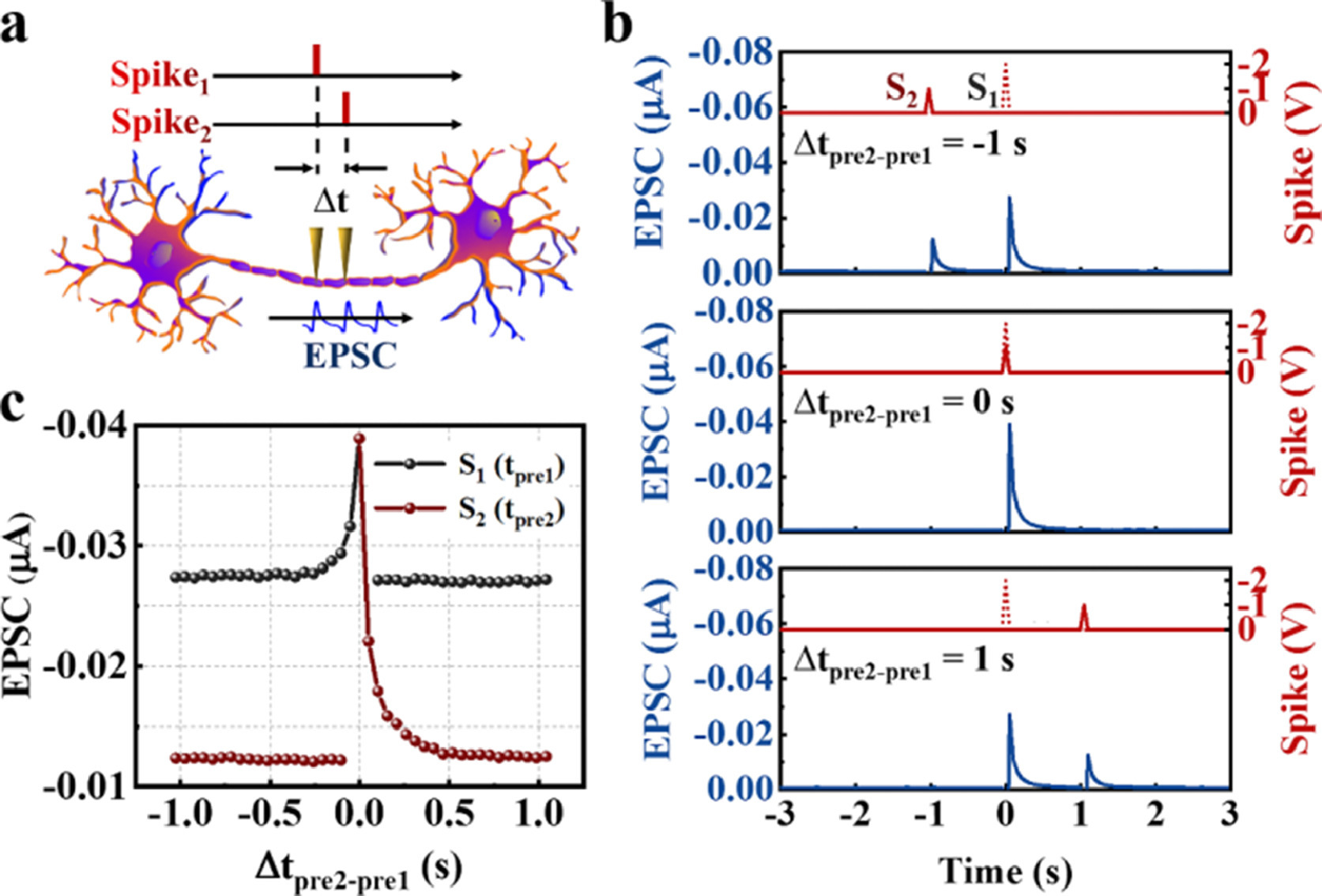
In nervous systems, dendrites can receive and process information from multiple synapses [37]. Multi-terminal inputs can apply a pair of spatiotemporally-correlated presynaptic spikes (S1: −2 V, 0.05 s; S2: −1 V, 0.05 s) onto the OAS (Fig. 4a); this possibility benefits the establishment of the dynamic logic in neural networks. To explore the effect of spatiotemporally correlated presynaptic spikes on a postneuron, we set the time node when spike S1 was triggered as t = 0. When S1 and S2 were applied sequentially, separated by an interval Δtpre2-pre1, the accumulation of migrated ions caused an increasing total amplitude of EPSC (Fig. 4b). EPSCs triggered by such two spikes varied with Δtpre2-pre1 (Fig. 4c). If S1 was applied later than S2, i.e., Δtpre2-pre1 < 0, EPSC at t = 0 was the superimposition of the second EPSC and the remaining first EPSC; Conversely, when S1 was applied earlier than S2, i.e., Δtpre2-pre1 > 0, the EPSC at t = 0 remained stable at the current peak triggered by S2, but the remained current induced by S1 was superimposed onto the S2-triggered EPSC. As Δtpre2-pre1 decreased, the superimposed current gradually increased. At Δtpre2-pre1 = 0, a maximum EPSC was triggered by the superimposition of two EPSCs at the same time.
Figure 4
Figure 4.
(a) Schematic of applying spatiotemporally correlated presynaptic spikes onto a postneuron through two presynaptic connections to one single strand of dendrite. (b) EPSCs triggered by S1 and S2 with Δtpre2-pre1 = −1 s, 0 s or 1 s. (c) EPSCs triggered by S1 and S2 as a function of Δtpre2-pre1.
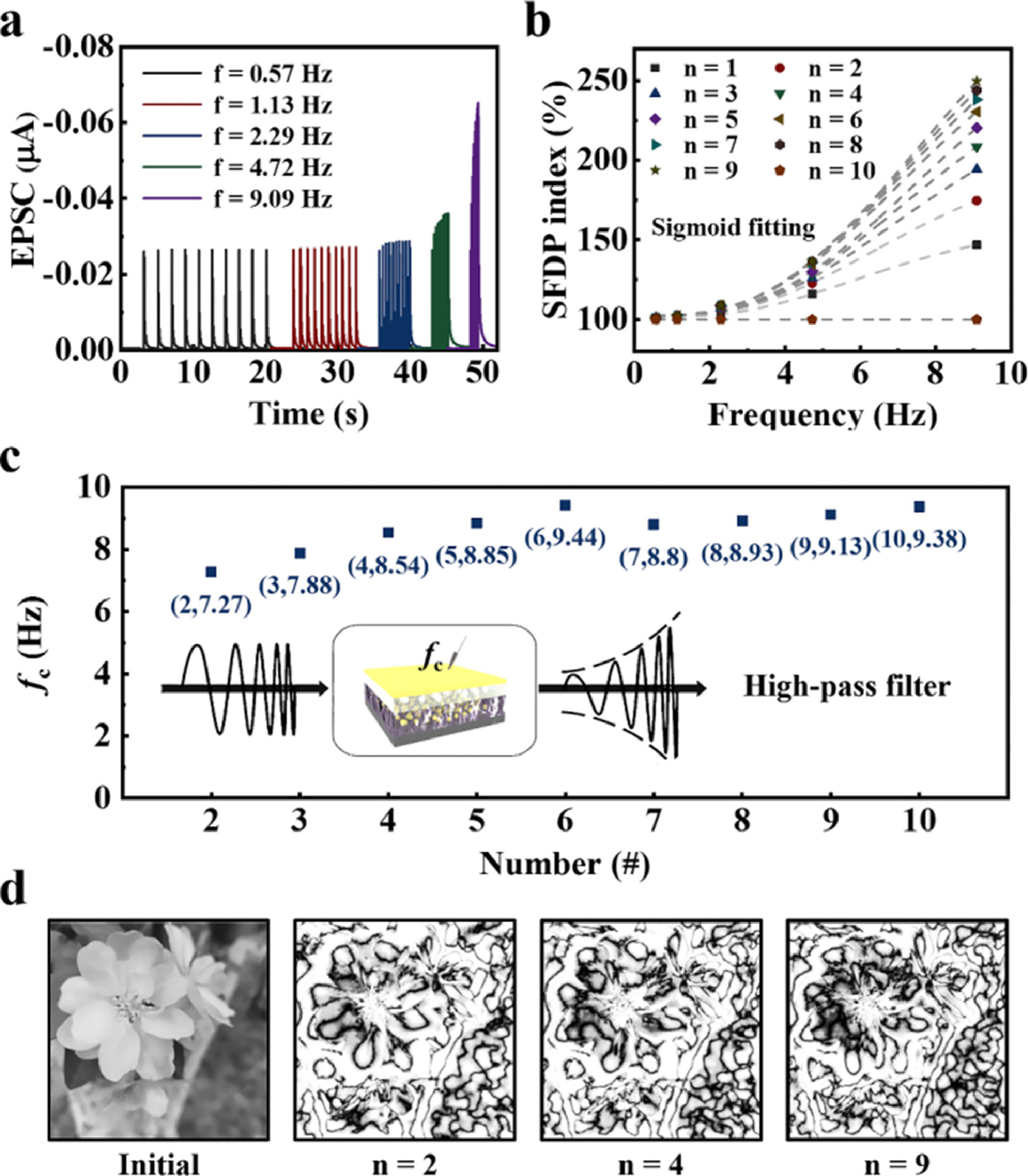
In biology, synapses with a low probability of neurotransmitter release yield a high-pass filtering effect [5]: They relay only signals that have a frequency f that exceeds a certain cut-off value fc, but greatly weaken other signals. To quantify the high-pass filtering behavior of our OAS devices, the EPSCs was characterized in response to stimulation using 10 successive presynaptic spikes that had 0.57 ≤ f ≤ 9.09 Hz (Fig. 5a). SFDP indexes (Af/A0.57 × 100%) under different n were also recorded (Fig. 5b). As f increased, EPSC also increased gradually. The dependence of EPSC gain on spike frequency was fitted using a sigmoidal function (Eq. 3) [8,38].
(3)
where p is the order of the function, a1 is the initial amplitude and a2 is the final amplitude. The fitting estimated fc = 7.27 Hz initially, and as n increased from 2 to 10, fc converged to ~9 Hz (Fig. 5c).
Figure 5
Figure 5.
(a) EPSCs triggered by different frequencies of spikes. (b) SFDP index according to the spike frequency, with different spike numbers. (c) fc regulated by different numbers of spikes for high-pass filtering. (d) Sharpening of an image of the flower by a dynamic filter with tunable fc.
To demonstrate the dynamic filtering function of the OAS device, an image of a flower was treated as an example to simulate the filtering process. Compared to the original image, the outline characteristic could be sharpened after filtering. Increase in n yielded increase in the number of image details that were outlined and highlighted, and a remarkable improvement was obtained (Fig. 5d).
We have presented a flexible organic artificial synapse that is fabricated using a one-step spin-coating process. The domain order of the blend organic layer can be modulated in a short range by varying the anion injection from chitosan film under different negative spikes, and this modulation can further adjust the transmission efficiency of hole carriers in vertical channels. Due to the mismatch of spatial domains in the organic blend film, the OAS device manifested strictly defined STP with a charge-retention time of only 49 ms, which is the shortest yet achieved. In flexibility tests, a 16 × 16 array of the devices retained 90.6% and 70.2% of its initial current level after 104 bending cycles at a radius of 8 mm and 1 mm, respectively; this is the best mechanical deformation endurance among current flexible two-terminal artificial synapses. The fc can be regulated by varying the number of presynaptic spikes applied to OAS devices; this process has a dynamic-filter characteristic, which can increase the detail in perceived images. This OAS device provides another resource towards neuromorphic time-frequency signal computing.
Declaration of competing interest
The authors declare that they have no known competing financial interests or personal relationships that could have appeared to influence the work reported in this paper.
Acknowledgment
This work was supported by the National Key R&D Program of China (Nos. 2022YFE0198200, 2022YFA1200044), the National Science Fund for Distinguished Young Scholars of China (No. T2125005), the Tianjin Science Foundation for Distinguished Young Scholars (No. 19JCJQJC61000), and the Shenzhen Science and Technology Project (No. JCYJ20210324121002008).
Supplementary materials
Supplementary material associated with this article can be found, in the online version, at doi:10.1016/j.cclet.2023.108419.
[1]
K. Yue, Y. Liu, R.K. L.ake, A.C. P.arker, Sci. Adv. 5 (2019) eaau8170. doi: 10.1126/sciadv.aau8170
Figure 1
(a) Schematic illustrations of an OAS device. (b) Cross-sectional SEM (left) and EDS (right) images of the tri-blend organic layer on a p-type Si substrate. (c) AFM images of P3HT:PMMA blend film (left), C8BTBT:PMMA blend film (middle) and tri-blend film (right). (d) Corresponding CPD of the tri-blend organic layer on a p-type Si substrate using the KPFM mode after top bias of 0 V (initial state), −4 V and 0 V (withdraw the top bias) on the AFM tip. (e) C-V curve of chitosan film. (f) Schematic diagram of device structure, ion migration and electric field distribution under bias.
Figure 2
(a) Schematic illustrations of a biological synapse. (b) EPSC triggered with a presynaptic spike (amplitude = −2 V, duration = 0.05 s) and a primordial potential of −0.1 V is applied. (c) The EPSCs measured with a pair of presynaptic spikes (amplitude = −2 V, duration = 0.05 s, and ∆t = 0.05 s). (d) PPF index plotted as a function of ∆t.
Figure 3
(a) EPSCs triggered by different numbers of presynaptic spikes (amplitude = −2 V, duration = 0.05 s). (b) SNDP index according to the number of presynaptic spikes, with different presynaptic spike amplitudes. (c) EPSC-retention curve of OAS after 100 presynaptic spikes (amplitude = −2 V, duration = 0.05 s). (d) EPSC-degradation rates according to the number of bending cycles to curvature radii of 8 mm and 1 mm, respectively.
Figure 4
(a) Schematic of applying spatiotemporally correlated presynaptic spikes onto a postneuron through two presynaptic connections to one single strand of dendrite. (b) EPSCs triggered by S1 and S2 with Δtpre2-pre1 = −1 s, 0 s or 1 s. (c) EPSCs triggered by S1 and S2 as a function of Δtpre2-pre1.
Figure 5
(a) EPSCs triggered by different frequencies of spikes. (b) SFDP index according to the spike frequency, with different spike numbers. (c) fc regulated by different numbers of spikes for high-pass filtering. (d) Sharpening of an image of the flower by a dynamic filter with tunable fc.


 DownLoad:

 下载:
下载:


