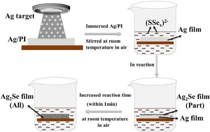
Figure 1.
Schematic illustration of the forming mechanism of β-Ag2Se thin film.
Scrutinizing the facile growth of β-Ag2Se fine films
Yongkang Ge , Yan Lei , Xu Li , Ruijuan Qi , Xiaoming Ma , Zhi Zheng

Thermoelectric (TE) material is a new type of functional semiconductor material which can directly convert thermal and electrical energy depending on the movement of carriers in the material. The thermoelectric energy conversion efficiency is mainly determined by the thermoelectric figure-of-merit value (zT = S2σT/κ). Except for Bi2Te3 used commercially today, the n-type chalcogenide Ag2Se also has similar properties, which is of high thermoelectric research value [1-4]. Ag2Se belongs to the silver chalcogenide group, which transitions from the low temperature orthorhombic phase (β) to the high temperature cubic phase (α) at temperatures close to 410 K [5-7]. Compared with the high temperature α-Ag2Se phase, the low temperature β-Ag2Se phase has higher thermoelectric properties, being proved to be a competitive candidate for n-type TE materials [8,9]. In addition, compared with traditional bulk thermoelectric devices, thin film thermoelectric cells not only save expensive processing steps and reduce material waste, but also can be made into the required size and shape, which can meet the needs of many narrow spaces and complex device structures [10-12]. So more researchers are exploring new synthetic methods to prepare β-Ag2Se thin films [13-16].
We reported previously a simple and efficient room temperature in-situ preparation method to synthesis β-Ag2Se thin film with high thermoelectric properties by direct metal surface element reaction (DMSER) solution processing selenization pathway. The in-situ synthetic method not only avoid high experiment temperature, laborious multistep procedures and the harsh experiment conditions, but also can control precisely the composition of products. In the typical process, the Ag film (~690 nm thick) was directly converted into pure phase β-Ag2Se film (~1 µm thick) with high [201] oriented columnar grains in only about 25 s [17]. However, the fast conversion of Ag to β-Ag2Se was not studied in depth, which is important to understand the reaction fundamental mechanism and provide the synthetic strategy to obtain the more fine films materials.
Herein, we further monitored and explored carefully the in-situ growth of β-Ag2Se fine films at different reaction time during the DMSER elemental selenization. Based on HASB theory and strong oxidation reaction mechanism, combined with XRD, SEM and TEM characterizations, we found that the β-Ag2Se fine films could be formed after the reaction of Ag film in Se/Na2S precursor solution for 1 s only. We demonstrated that the formation of β-Ag2Se thin films is in a growth driven mode with no obvious orientation or growth rate selections to the sputtered elemental Ag films. With the increase of reaction time, β-Ag2Se grew directly from the surface of Ag film to the interface between Ag film and PI, until completely reacted into dense large columnar crystals. From the beginning to the end of the reaction, there is no formation of impurities and the prepared β-Ag2Se film is flat and uniform, which once again verifies the preciseness and accuracy of our previous work.
In this study, the forming mechanism of β-Ag2Se thin film could be prepared following the schematic illustration in Fig. 1. Our research group has reported that the final product β-Ag2Se was pure phase through this preparation method in the previous work [17]. In the present work, Se/Na2S mixed solution contains many ions and its material balance is difficult to study. Through consulting literature materials [18-21], the possible reaction mechanism is as follows:
|
|
(1) |
|
|
(2) |
where x of (SSex)2− is greater than or equal to 2. Firstly, the dissolution of Se powder can be obviously observed in Na2S mixed solution, and the color of solution changes from colorless to black red with the increase of the dissolution of Se powder. During the process of dissolution, the selenium element interacts with S2− in the aqueous solution to form selenium sulfur anion, which has more active and stronger oxidation ability, similar to peroxyanion or superoxide anion [22]. Subsequently, the sputtered elemental Ag can spontaneously react with Se or S (chalcogenide elements) to form Ag2Se or Ag2S. Therein, the calculated chemical hardness of Ag was 3.21, which belonged to soft base, and the chemical hardness values of soft acid S and Se were 4.05 and 3.73, respectively. Based on the HSAB theory, the formation rate of Ag2Se compounds is faster than that of Ag2S [23,24]. So, a large area Ag film can be converted to Ag2Se without Ag2S impurity by the low-temperature in-situ method [17].
To understand the process of the fast conversion of β-Ag2Se from the elemental Ag, samples with different reaction times were characterized as follows. Fig. 2a and Fig. S1 (Supporting information) show that the samples were divided into 6 groups (1–25 s) with the reaction time as the variable and characterized respectively by XRD. The samples are compared with the standard cards of Ag2Se (No. 24–1041) and Ag (No. 87–718). As shown in Fig. 1a, except for the diffraction peaks of Ag, the (121) and (201) diffraction peaks of Ag2Se appear after the sputtered Ag being immersed in Se/Na2S mixed solution for 1 s, indicating that a part of Ag has already been converted into β-Ag2Se on the Ag thin film surface, although the content of Ag is still large at this time. During the reaction period of 5–20 s, the peak intensity of Ag gradually becomes weaker, while that of Ag2Se becomes stronger, indicating that the thickness of Ag2Se gradually increased, and the content of Ag gradually decreased. When the reaction time reaches 25 s, the Ag peak signal has disappeared thoroughly, while Ag2Se diffraction peaks without other impurity peaks are consistent with those of Ag2Se standard card. It worth noting that during reaction 1–10 s, β-Ag2Se was formed at this time, but exhibited no preferential orientation. The priority of growth along (121) and (201) crystal planes was roughly similar. Until after 10 s reaction, the preferred crystal orientation of β-Ag2Se was along (201) lattice planes [17].
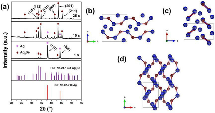
The variation of the β-Ag2Se crystal growth orientation may be attributed to the transport of the Ag atoms during the in-situ conversion of Ag to β-Ag2Se. As shown in Figs. 2b-d, there are Ag-Se-Ag-Se atom-chains and single Ag atom in the β-Ag2Se crystal. The channels in the crystal structure can be observed along both the a and b axes, where the Ag atoms may be transported. However, there are some differences in these two channels. Primarily, along b axis, the S sharp Ag-Se-Ag-Se atom-chains block the transport of Ag atoms to a certain degree. In other words, these channels are not suitable for the transport of Ag atoms during the reaction at RT. Interestingly, different from the channels along b axis, the channels along a axis are more suitable for Ag atoms' transport. These above results indicate that the (100) planes are the preferred planes in theory in our work. Notably, (201) planes are close to (100) planes with an angle of 15.58°, which may be the reason for the special growth direction normal to (201) planes.
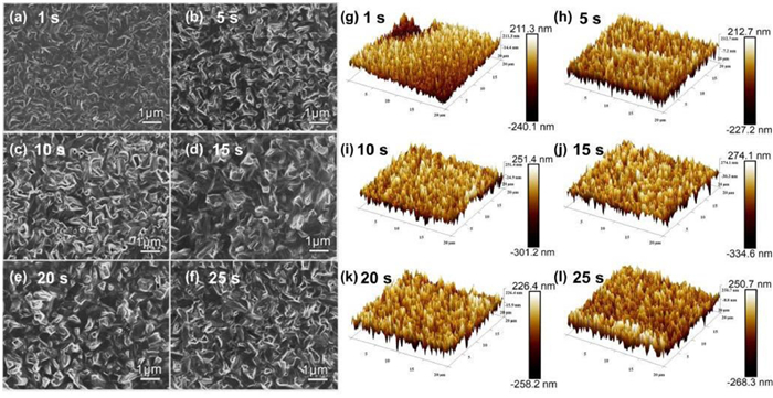
In order to verify the elemental valence of the final product (at 25 s) of the reaction, XPS test was further performed. Figs. S2a and b (Supporting information) show the binding energy of Ag (3d3/2, 3d5/2) emerged at 368 eV and 375 eV, suggesting that the oxidation state of Ag was univalent Ag+ in thin film. As for Se element, Se (3d3/2, 3d5/2) located at 53 eV and 55 eV, suggesting that the oxidation state of Se was univalent Se2− in thin film. These results indicate that the valence states of Ag and Se in the films are consistent with those of pure β-Ag2Se. From the SEM images (Figs. 3a-f), compared with the dense surface of the unreacted Ag film [17], holes appear on the surface of the film after 1 s reaction, indicating that part of Ag has already converted to β-Ag2Se. As the reaction time increase, we can find that the crystal sizes and morphology of β-Ag2Se are almost the same, but there are little pin-holes in the β-Ag2Se thin films, indicating the β-Ag2Se products gradually become well compactness. Similarly, from the AFM images (Figs. 3g-l), it was found that the height of the middle region was inconsistent with that of the two sides at 1 s, indicating that some Ag was reacted. The crystal surface shape at each time period was roughly similar to that of SEM image, and the formed films became more and more uniform and flat with the increase of the reaction time. XRD, SEM and AFM indicate that the reaction rate of Ag in Se/Na2S precursor solution is extremely high, and the surface of prepared β-Ag2Se film is flat and uniform, implying it is in a growth driven mode.
The crystal growth kinetics of β-Ag2Se from the elemental Ag in the Se/Na2S solution should be either nucleation driven or growth driven. Next, to further explore the microscopic origin of crystallization kinetics of β-Ag2Se from elemental Ag, the cross-sectional TEM images of the β-Ag2Se thin film growth at 1 s, 10 s and 25 s have been measured and illustrated in Figs. 4a-c, as well as the EDS mappings of element Ag, Se (Figs. 4d-l). We can clearly observe the uniform and flat interface between the β-Ag2Se and Ag, suggesting that this reaction occurred from top to the bottom of the samples with consistent reaction rate for different Ag grains, following the growth driven mode with very fast crystal growth rate and no sizeable and robust crystalline seeds form during the short timescale involved in the growth process. Taking sample at 1 s as an example. It is obvious from the Ag or Se elemental image that there are two parts with different color depths. The upper part of the Ag image with light color and the upper part of the Se image with deep color are both β-Ag2Se, whereas the lower part of them is mostly Ag simple substance that has not been reacted. The elemental images of Ag or Se of samples at 10 s and 25 s are similar to it, except that the content of Ag simple substance decreases with time, and Ag has been completely replaced by β-Ag2Se at 25 s. It can be found that, part of the Ag has been already converted into β-Ag2Se at 1 s, and β-Ag2Se has occupied a dominant content at 10 s. This reaction can finish within about 25 s, which is consistent with XRD results. As the increase of the reaction time, the columnar β-Ag2Se crystal gradually formed, and this structure was conducive to improving the thermoelectric properties of material. In this process, the thickness of the initial Ag film to β-Ag2Se formed (at 25 s) increased from about 690 nm to about 1 µm. Combined with the above characterizations, when Ag reacts in Se/Na2S precursor solution for 1 s, its surface morphology is very close to that of pure β-Ag2Se, and β-Ag2Se is formed by rapid direct growth from the surface of Ag film to the interface between Ag film and PI during the reaction process [25]. Figs. 4m and n are the cross-sections and top-view of TEM images of sample at 1 s. It can be clearly seen that there are two parts with different color depths, β-Ag2Se and Ag respectively, and their boundaries have been marked with red dotted lines. It is verified again that β-Ag2Se has been generated in 1 s. Figs. 4p-q are the HRTEM image of sample at 1 s and its local magnified image, which clearly shows the lattice stripes of β-Ag2Se and Ag.

The lattice spacing of β-Ag2Se and Ag is 0.210 nm and 0.231 nm respectively, which correspond to the crystal plane (201) of β-Ag2Se and the crystal plane (111) of Ag respectively, which further proves that β-Ag2Se grows along (201) crystal plane. To further verify the thermoelectric properties of β-Ag2Se (samples at 25 s reaction time) thin films at room temperature, we obtained the values of mobility, carrier concentration and Seebeck coefficient through instrument tests. Compared with state of art reports on the thermoelectric properties of β-Ag2Se films (Figs. 4r and s, Table S1 in Supporting information), it is found that the β-Ag2Se films prepared in this work possess better thermoelectric properties [14,17,26-28]. The properties in this work are similar to the best of our previous work, combined with the above characterizations, it is further verified that the β-Ag2Se thin film are generated by above method was conducive to phonon scattering and carrier transmission [27], and effectively improves the thermoelectric properties [17,29].
To explore the microscopic origin of crystal growth kinetics with the aim to improve the TE properties of β-Ag2Se films, we have carried out time-dependent investigation in the quality and thickness control for β-Ag2Se films. Based on HSAB theory and strong anion oxidation and the comprehensive analyses, we demonstrated that the formation of β-Ag2Se film is in a growth driven mode without orientation or reaction rate selections to the Ag precursor in Se/Na2S solution, which attributed to the obvious conversion of a uniform and flat β-Ag2Se fine film on the Ag precursor for 1 s only. The (201) crystal planes of β-Ag2Se became the preferred orientation after 10 s reaction. In the whole reaction growth process, β-Ag2Se grew directly from the surface of Ag film to the interface between Ag film and PI, meanwhile, the structure of β-Ag2Se generated in 1–25 s was always very dense. Additional part of thermoelectric properties measured in this work, it is verified again that the structure of the thin film optimizes the electrical and thermal conductivity, which greatly improves the thermoelectric properties. The room temperature in-situ preparation strategy for β-Ag2Se TE films could pave a new avenue to promote the development of thermoelectric materials at RT in air, as a complementary approach to current nanotechnology.
The authors declare that they have no known competing financial interests or personal relationships that could have appeared to influence the work reported in this paper.
We are grateful for the financial support provided by National Natural Science Foundation of China (Nos. 52072327, 21673200, 21877027, 61504117, U1604121), Zhongyuan Scholars Program of Henan Province, China (No. 20210151004), Youth Talents Lifting Project of Henan Province, China (No. 2018HYTP010), and Key Research and Development Project of Henan Province, China (No. 192102210183).
Supplementary material associated with this article can be found, in the online version, at doi:
G.J. Snyder, E.S. Toberer, Nat. Mater. 7 (2008) 105–14. doi: 10.1038/nmat2090
X. Shi, J. Yang, J.R. Salvador, et al., J. Am. Chem. Soc. 133 (2011) 2842.
M. Ferhat, J. Nagao, J. Appl. Phys. 88 (2000) 813. doi: 10.1063/1.373741
W.L. Mi, P.F. Qiu, T.S. Zhang, et al., Appl. Phys. Lett. 104 (2014) 133903. doi: 10.1063/1.4870509
M.C. Santhosh Kumar, B. Pradeep, Mater. Sci. 25 (2002) 407–411.
K.X. Zhou, J.K. Chen, R.K. Zheng, et al., Ceram. Int. 42 (2016) 12490-12495. doi: 10.1016/j.ceramint.2016.05.037
P.P.J. Helan, K. Mohanraj, G. Sivakumar, T. Nonferr. Metal. Soc. 25 (2015) 2241–2246.
C. Lee, Y.H. Park, H. Hashimoto, J. Appl. Phyl. 101 (2007) 024920. doi: 10.1063/1.2429727
M.C. S. anthosh Kumar, B. Pradeep, Mater. Lett. 56 (2002) 491–495. doi: 10.1016/S0167-577X(02)00538-4
E.D. Kolb, R.A. Laudise, J. Appl. Phys. 42 (1971) 1552–1554. doi: 10.1063/1.1660338
N. Jaziri, A. Boughamoura, J. Müller, et al., Energy Rep. 6 (2019) 264–287.
Q.H. Zhang, X.Y. Huang, S.Q. Bai, et al., Adv. Eng. Mater. 18 (2016) 194–213. doi: 10.1002/adem.201500333
T. Day, F. Drymiotis, T.S. Zhang, et al., J. Mater. Chem. C 1 (2013) 7568–7573. doi: 10.1039/c3tc31810a
C. Jiang, Y.F. Ding, K.F. Cai, et al., ACS. Appl. Mater. Interface 12 (2020) 9646–9655. doi: 10.1021/acsami.9b21069
S. Jindal, S. Singh, G.S.S. Saini, et al., Appl. Phys. A: Mater. 126 (2020) 374. doi: 10.1007/s00339-020-03534-1
E. Fernández-Díaz, A.B. Espinoza-Martinez, A. Flores-Pacheco et al., J. Electron. Mater. 48 (2019) 3405–3409. doi: 10.1007/s11664-019-07104-x
Y. Lei, R.J. Qi, M.Y. Chen, et al., Adv. Mater. 34 (2021) 2104786.
J.Q. Hu, Q.Y. Lu, K.B. Tang, et al., Chem. Commun. (2000) 715–716.
E. Protopopoff, P. Marcus. Electrochim. Acta 63 (2012) 22–27. doi: 10.1016/j.electacta.2011.12.030
J. Ortíz-Corona, F.J. Rodríguez-Gómez. T. Nonferr. Metal. Soc. 29 (2019) 2646–2657. doi: 10.1016/S1003-6326(19)65171-X
Q. Peng, Y.J. Dong, Z.X. Deng, et al., Inorg. Chem. 41 (2002) 5249–54. doi: 10.1021/ic0257266
J.S. Valentine, A.B. Curtis, J. Am. Chem. Soc. 97 (2002) 224–226.
D.W. Yang, X.L. Su, F.C. Meng, et al., J. Mater. Chem. A. 5 (2017) 23243–23251. doi: 10.1039/C7TA08726H
H.Z. Duan, Y.L. Li, K.P. Z. hao, et al., Jom-Us. 68 (2016) 2659–2665. doi: 10.1007/s11837-016-1980-4
Z.H. Zheng, D.L. Zhang, J.Y. Niu, et al., Mater. Today Energy. 24 (2022) 100933. doi: 10.1016/j.mtener.2021.100933
J.A. Perez-Taborda, O. Caballero-Calero, L. Vera-Londono, et al., Adv. Eng. Mater. 8 (2018) 1702024. doi: 10.1002/aenm.201702024
N. Chen, M.R. Scimeca, S.J. Paul, et al., Nanoscale Adv. 2 (2020) 368–376. doi: 10.1039/c9na00605b
Y.F. Ding, Y. Qiu, K.F. Cai, et al., Nat. Commun. 10 (2019) 841. doi: 10.1038/s41467-019-08835-5
N. Nandihalli, Mater. Today Energy. 25 (2022) 100965. doi: 10.1016/j.mtener.2022.100965

Figure 2 (a) XRD patterns of the fabricated β-Ag2Se with different reaction time (1 s, 10 s and 25 s). (b-d) β-Ag2Se crystal structure view along a, b and c axis (Ag atoms marked with Ag1 form the channels for Ag atoms transport).

Figure 3 (a-f) SEM images of β-Ag2Se with different reaction time. (g-l) AFM images of β-Ag2Se with different reaction time.

Figure 4 (a-c) The cross-sectional TEM images of the β-Ag2Se thin film growth at 1 s, 10 s and 25 s. (d-l) EDS maps of elements Ag and Se corresponding to 1 s, 10 s and 25 s samples. (m) The cross-sectional TEM image of the β-Ag2Se thin film at 1 s. (n, o) TEM and HRTEM images of the interface between β-Ag2Se and Ag phases at 1 s. (p, q) Enlarged HRTEM image of the orange square marked in (o). (r, s) Comparison of thermoelectric properties between this work (samples at 25 s reaction time) and literatures.

 扫一扫看文章

扫一扫关注我们
 DownLoad:

 下载:
下载: