
Figure 1.
Five performance parameters of high-performance OFETs and typical methods to improve them.
High-performance and multifunctional organic field-effect transistors
Yujie Zhao , Wei Wang , Zihan He , Boyu Peng , Chong-An Di , Hanying Li

Field-effect transistors are the central components of the modern silicon-based microelectronics industry. However, restricted by the quantum tunneling effects, it becomes increasingly difficult for the silicon-based field-effect transistors to further approach smaller dimensional. It was thus of great research and industrial interests to explore new semiconductor technologies that can promote the performance and/or broaden the functionality of the field-effect transistors. Ⅲ-V tunnel field effect transistors [1], two-dimensional materials [2], carbon nanotubes [3,4], metal oxides [5,6], etc., are representative materials that have shown their strength.
Among the emergent semiconductor techniques, organic semiconductors have received extensive attention from global researchers for the projects in flexible electronics and diverse functional devices like sensors. Since the advent of the first organic field-effect transistor in 1986 [7], tremendous efforts have been made toward implementation of high-performance OFETs and its application. Compared with their inorganic counterparts, OFETs have the advantages of diversified processing methods, low processing temperature, wide selection of materials, and compatibility with flexible substrates and roll-to-roll fabrication.
With the continuous development, the performance of OFETs has been greatly improved. As one of the most crucial parameters, mobility has been improved from 10−5 cm2 V−1 s−1 in the 1980s to over 20 cm2 V−1 s−1 now [8-10]. At the same time, in order to achieve energy-efficient OFETs, other performance parameters such as threshold voltage, subthreshold swing and contact resistance have also been greatly developed in recent years. For example, Wang et al. combined organic monolayer crystals, ferroelectric gate dielectrics and van der Waals device integration [11]. In addition to a highest mobility of more than 10 cm2 V−1 s−1, the OFETs also achieved close-to-zero threshold voltage, subthreshold swing of sub-60 mV/dec and contact resistance below 60 Ω cm. Furthermore, the stability of OFETs, especially the bias stress stability, has also been extensively explored to realize practical applications [12,13].
In particular, OFETs have a wide range of functional applications since weak perturbations in the conducting channel can cause very dramatic performance changes [14,15]. The multifunctional OFETs not only benefit from the excellent optoelectronic properties and sensing properties of organic materials, but also the three-terminal device configuration of OFETs is advantageous for signal amplification of external stimuli. Thus, the OFET is a good carrier for functional applications, and a series of functional devices have been realized successfully, including OFET-based sensors [16-18], organic light-emitting transistors (OLETs) [19,20], memory devices [21], artificial synapses [22] and adaptive devices [23].
Herein, this review starts from high-performance OFETs from the perspective of performance parameters including mobility, threshold voltage, subthreshold swing, contact resistance and bias stress stability. Next, we concentrate on recent advances about multifunctional OFETs, which contain OFET-based sensors, OLETs, memory devices, artificial synapses and adaptive devices. Finally, the challenge and possible future development for the OFETs are presented.
Typical OFETs consist of three electrodes (source, drain and gate), dielectric and organic semiconductor. The basic principle of OFETs is to control the channel current between the source and drain electrodes (IDS) by changing gate voltage (VG). The gate voltage induces electrical field through the gate dielectric and accumulates carriers at the interface between the organic semiconductor and gate dielectric. Depending on the high or low density of the accumulated carriers, the OFET device is in ON or OFF state. The transfer characteristic curves (IDS versus VG) and output characteristic curves (IDS versus VD) are the most basic performance of any OFETs. From these two critical I-V curves, key information including mobility (µ), threshold voltage (Vth), subthreshold swing (SS), Ion/Ioff ratio, etc., can be attained.
Among the studies in the research field of OFETs, a significant portion was focusing on advancing the electrical performance as it is the cornerstone for realizing the practical application of OFETs in various aspects. In this section, we will discuss several key figures of merits of OFETs and summarize recent research progress on how to improve them. As shown in Fig. 1, this section mainly includes five parts: high mobility, low threshold voltage, low subthreshold swing, low contact resistance and long-term bias stress stability.
In all field-effect transistors including OFETs, mobility is the most fundamental parameter as it determines the switching speed of the device. Mobility depends on many factors such as the molecular structure of semiconductors, the morphology of semiconductor film, device structure, trap density and process condition. The development of high-mobility OFETs focus on new materials and methods. The aspect of new materials is not presented in this review as it has been well summarized in previous reviews [10,24,25]. For methods to improve mobility, we mainly illustrate from the following five respects: (1) controlling molecular packing; (2) crystal alignment; (3) doping of organic semiconductor; (4) post-treating of the device; (5) interface engineering.
Compared with organic thin films, organic crystals show higher mobility because of fewer structural defects like trap density and grain boundaries [26,27]. Most reported high-mobility organic transistors are based on organic semiconductor single crystals [28,29]. However, due to weak non-directional intermolecular interactions between organic semiconductor molecules, there are two or more polymorphs in organic semiconductor crystals. Polymorphs usually result in greatly varying mobility owing to the different intermolecular distances and positions [30,31].
By physical vapor transport (PVT) method, Hu's group obtained two phases of titanyl phthalocyanine (TiOPc) crystals by controlling the temperature [32]. The α-phase crystals exhibited 2D lamellar brickstone motif with maximum mobility up to 26.8 cm2 V−1 s−1. In sharp contrast, the mobility of β-phase crystals with an unusual 3D framework was only 0.1 cm2 V−1 s−1 (Figs. 2a and b). Theoretical calculations demonstrated that the much lower mobility of β-phase crystals is caused by the destructive interference effects of inter-layer electronic coupling pathways perpendicular to charge transport direction. Similarly, by varying the solution concentration, He and coworkers obtained α-phase and β-phase single crystal of dihexyl-dibenzo[d, d']thieno[3, 2-b; 4, 5-b']dithiophene (C6-DBTDT) in the drop casting method [33]. The highest mobility of α-phase and β-phase single crystal is 18.9 cm2 V−1 s−1 and 8.5 cm2 V−1 s−1, respectively.

Apart from these two examples, many other organic semiconductors such as N, N′-bis-(heptafluorobutyl)-2, 6-dichloro-1, 4, 5, 8-naphthalene tetracarboxylic diimide (Cl2-NDI) [34] and 2-dodecyl[1]benzothieno[3, 2-b][1]benzothiophene (BTBT-C12) [35] can also achieve high mobility by tuning the polymorphism. Additionally, the phenomenon of polymorphs also exists in conjugated polymers. Li et al. obtained two semi-crystalline phases of a diketopyrrolopyrrole (DPP) based polymer by precisely controlling the solvent [36]. β1-phase was prepared from pure chloroform, while β2-phase could be obtained when a small amount of 1, 2, 4-trichlorobenzene was added. OFETs based on the β2-phase showed 4-fold higher mobility as a result of reduced π-π stacking distance. Aside from tuning the crystal polymorphs via self-assembly, providing external force is another technique to modulate molecular packing. As a classic example, Bao's group induced lattice strain by regulating the speed in solution shearing method [37]. With increasing shearing speed, the π-π stacking distance of 6, 13-bis(triisopropylsilylethynyl)pentacene (TIPS-pentacene) reduced from 3.33 Å to 3.08 Å (Figs. 2c–f). Strained films exhibited a maximum mobility of 4.6 cm2 V−1 s−1 while the mobility of unstrained films was only 0.8 cm2 V−1 s−1 (Figs. 2g and h). Furthermore, they used fluid-enhanced crystal engineering (FLUENCE) to manipulate crystal morphology. And non-equilibrium crystal lattices were obtained by lowering solution concentration, which avoided crystal defects introduced by high shearing speed [38]. The OFETs of TIPS-pentacene film with both non-equilibrium crystal lattices and controlled morphology showed maximum mobility of 11 cm2 V−1 s−1. Besides, alternating electric fields can also alter the organic semiconductor crystal packing [39]. The mobility of TIPS-pentacene had a twofold enhancement after introducing electric fields, but the mobility of 2, 7-dioctyl[1]benzothieno[3, 2-b][1]benzothiophene (C8-BTBT) decreased by a factor of three.
The previous section presents the importance of controlling the molecular packing structure. Moreover, since organic crystals have different intermolecular interactions in different directions, their charge transport tends to be anisotropic, that is, mobility varies along different directions. So how to make organic crystal alignment an important research field [40-42].
Among the numerous methods for preparing organic semiconductor crystals, the meniscus-guided coating (MGC) techniques is widely used because it can quickly prepare large-area crystals with good uniformity and is compatible with roll-to-roll processes. Typical MGC techniques includes slot die coating, zone casting, dip coating, blade coating and bar coating. Due to the inherent directionality of MGC techniques, it can easily induce aligned crystals [43,44]. Lee et al. used bar coating method shown in Fig. 3a to prepare C8-BTBT crystals. The OFETs fabricated with this exhibited a highest mobility of 20.6 cm2 V−1 s−1 [45]. In this work, they first got a reasonable coating speed of 1–2 mm/s through systematic experiment. Then wettability-patterning substrate was prepared to obtain highly aligned single-crystal-like film. Specifically, by creating an appropriate difference in surface energy between the wetting and non-wetting areas, the solution maintained a high contact angle along the rim of the pattern, which prevented polycrystalline behavior brought by undesired nucleation sites (Figs. 3c and d). In addition, they designed a pentagon shaped pattern in the initial coating region. The highly aligned single crystal film was produced by optimizing the nucleation spot angles between 35° and 60° (Fig. 3b). Furthermore, a mixed solvent of toluene and DMF was applied to introduce solutal Marangoni flow, which could provide enough solute to the contact line to form uniform OSC film. In brief, speed regulation, substrate patterning, and solvent engineering were used in this study to generate highly orientated and highly aligned organic semiconductor films. Additionally, MGC techniques can also be utilized in conjugated polymers [46]. Geng's group obtained uniaxially aligned film of polymer poly[2, 5-bis(4-tetradecyloctadecyl)pyrrolo[3, 4-c]pyrrole-1, 4(2H, 5H)‑dione-alt-5, 5′-di(thiophen-2-yl)-2, 2′-(E)-1, 2-bis(3, 4-difluorothien-2-yl)-ethene] (P4FTVT-C32) with larger fibrous structures by controlling coating speed [47]. The OFETs obtained a highest electron mobility of 9.38 cm2 V−1 s−1 by incorporation of polyethylenimine ethoxylated (PEIE) layer as electrode modification layer.
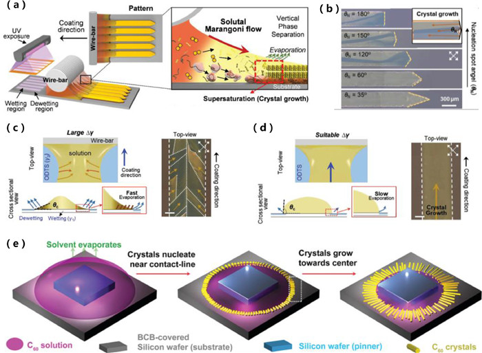
Aside from MGC techniques, another intriguing way to prepare aligned crystals is the improved drop casting methods, which include capillary tube method, inclined substrate method, droplet-pinned crystallization (DPC) method and so on. Here we briefly introduce DPC method because of its wide applicability and potential application prospects [48]. In 2012, Li et al. placed a small silicon wafer in the substrate's center to prevent the droplet from sliding. Thereby they created a steady contracting contact line and obtained well-aligned crystals along the droplet retreating direction [49]. The crystallization process is illustrated in Fig. 3e. In this way, well-aligned C60 single crystal with an electron mobility as high as 11 cm2 V−1 s−1 was prepared.
Doping is an effective way to improve mobility as it can tune the carrier concentration and fill trap states. However, due to the low doping efficiency of molecular dopants, the incompletely defined doping mechanism and the impact of dopants on semiconductor morphology, the doping of organic semiconductors is still in its infancy compared to the mature silicon-based doping techniques [50,51]. So here we simply introduce two studies on high-mobility OFETs through doping.
Paterson and co-workers added Lewis acid Zn(C6H5) as an additive to the active layer of OFETs. The mobility of C8-BTBT was significantly improved from 1.9 cm2 V−1 s−1 to 21.5 cm2 V−1 s−1 when the Zn(C6H5) concentration was just 0.025 mol% [52]. They demonstrated that Zn(C6H5) not only functioned as a p-type dopant, but also strongly affected the microstructure of the film. In detail, the addition of Zn(C6H5) resulted in the formation of smaller C8-BTBT lattices and larger molecular terraces, which contributed to the improved hole transport. In contrast to the in vivo doping of the semiconductor film described above, Heeger's group demonstrated that chemical vapor treatment could also result in doping at the metal/semiconductor interface [53]. When the devices of polymer poly[4-(4, 4-dihexadecyl-4H-cyclopenta[1, 2-b: 5, 4-b′]dithiophen-2-yl)-alt-[1, 2, 5]thiadiazolo-[3, 4-c]pyridine] (PCDTPT) were exposed to NH3 vapor, the positive charge at the metal/semiconductor interface was compensated and the threshold voltage moved from about 7 V to nearly 0 V. Whereas, the mobility increased to 58.6 cm2 V−1 s−1 when exposed to I2 vapor, which is frequently employed as a p-type dopant.
Solution processability is a major advantage of organic semiconductors. But the solvent inevitably remains in the interface and active layer, which may impede carrier transport. Thermal annealing is a typical method to avoid the impact of these residual solvents. Li's group demonstrated by X-ray photoelectron spectroscopy (XPS) that a trace amount of polar solvent molecules existed in the solution-processed crystals [54]. The OFETs based on 6, 13-bis(triisopropylsilylethynyl)-5, 7, 12, 14-tetraazapentacene (TIPS-TAP) crystals attained a greatest electron mobility of 13.3 cm2 V−1 s−1 after eliminating the residual polar solvent by thermal annealing. In addition to getting rid of leftover solvent, thermal annealing may also affect the microstructure of the film. Hiroaki et al. noticed that the step structure transformed from a 2.8 nm monolayer to a 5.7 nm bilayer when 2-decyl-7-phenyl-[1]benzothieno[3, 2-b][1] benzothiophene (Ph-BTBT-10) film was annealed at 120 ℃ for 5 min. This observation was validated by X-ray diffraction (XRD) and atomic force microscope (AFM) analysis (Figs. 4a–c). They attributed this phenomenon to the crystal-to-crystal phase transition during thermal annealing [55]. Following this annealing, device mobility was dramatically improved from 2.1 cm2 V−1 s−1 to 14.7 cm2 V−1 s−1 (Fig. 4d). Analogously, C8-BTBT polycrystalline films could be accurately tuned to bilayer or monolayer single crystals by controlling the annealing temperature [56]. The OFETs based on bilayer single crystals exhibited a highest mobility of 12.8 cm2 V−1 s−1.

In contrast to thermal annealing, solvent vapor annealing (SVA) partially dissolves semiconductors using saturated solvent vapors. In this way, SVA promotes the rearrangement of organic molecules, improves the morphology of thin film, and thus increases carrier mobility. Liu and coworkers illustrated that SVA could convert C8-BTBT thin film into 1D single crystals on dielectric poly(methyl methacrylate) (PMMA) [57]. The highest mobility of OFETs based on the 1D single crystal could reach 9.1 cm2 V−1 s−1.
The strategies used to increase carrier mobility in the paragraphs above are focused on improving active layers. Differently, this part predominantly focuses on the impact of the interface in OFETs. Interfaces in OFETs include the electrode-semiconductor interface and the semiconductor-dielectric interface. The electrode-semiconductor interface mainly affects the carrier injection, which will be discussed in the contact resistance section. The semiconductor-dielectric interface is critical for OFETs because it is generally accepted that charge carriers are transported within several molecular layers adjacent to the dielectric layer. Many interface properties, such as charge trap density, roughness, surface energy, strongly affect device performance. Here we introduce several reports on obtaining high-mobility OFETs through interface engineering. For more details, please refer to other reviews [57-59].
Polymer insulators are commonly utilized as dielectric layers in OFETs due to their inherent flexibility, variety of materials, and simple processing methods. However, since polymers cannot be purified by sublimation like small molecules, impurities are likely to be present in the dielectric layers, which will affect device performance. Meng's group developed supercritical CO2 fluids (SCCO2) for treating poly(vinyl alcohol) (PVA) to boost dielectric performance [60]. Mechanistic studies by XPS spectra have shown that SCCO2 could effectively eliminate mobile Na+ ions and reduce hydroxyl groups within PVA (Figs. 4e and f). Thence, the flexible OFETs based on C8-BTBT and SCCO2-treated PVA realized a very high hole mobility of 30.2 cm2 V−1 s−1.
Apart from a direct improvement on insulating layers to improve interfacial quality and device performance. Another method is to improve device performance through semiconductor-dielectric interactions. Ji et al. obtained quasi-monolayer pentacene film with orthorhombic phase on the dielectric layer poly(amic acid) (PAA) [61]. The experiments and theoretical simulations showed that there was a hole accumulation layer existed within the pentacene film, which was caused by the electron transfer from pentacene to PAA. Consequently, pentacene-based OFETs displayed an enhanced mobility to 13.7 cm2 V−1 s−1.
Threshold voltage is the minimum gate voltage to create a conducting path between the source and drain terminals. The lower threshold voltage means lower power consumption is needed to operate OFETs. Threshold voltage is used for overcoming the barrier between the electrode and the semiconductor and filling the carrier traps in the channel. Thereby, low threshold voltage can be achieved by minimizing the contact barrier and carrier traps. However, these two methods are usually also related to other parameters, which ought to be covered in the following sections. Here we introduce two more approaches to achieve low threshold voltage.
|
|
(1) |
where Dit is the interface trap state density and Ci is the unit-area capacitance of the dielectric. According to the equation, larger Ci is beneficial to reduce the influence of interface trap states, which naturally minimizes Vth. Ci can be calculated by Eq. 2:
|
|
(2) |
where k is the dielectric constant of the dielectric layer, ε0 is the dielectric constant of the vacuum, and d is the thickness of the dielectric layer. Therefore, increasing dielectric constant and decreasing thickness is useful for obtaining larger Ci.
Wang's group obtained Al2O3 dielectric layer with the capacitance of about 120 nF/cm2 at a relatively low temperature [63]. Based on this, OFETs of p-type semiconductor pentacene and n-type semiconductor N, N′-ditridecylperylene-3, 4, 9, 10-tetracarboxylic diimide (PTCDI-C13) achieved absolute threshold voltage value of less than 1 V. Walser et al. achieved capacitance value of about 100 nF/cm2 with an ultrathin fluoropolymer Cytop and its gate leakage current was less than 10 pA even with sub-20 nm thickness [64]. On the basis of this dielectric, the threshold voltage of PTCDI-C13-based OFETs was as low as 0.2 V. Apart from the two illustrative cases above, more other reported OFETs with large Ci dielectric can be found in other reviews [65-67]. Furthermore, another method to achieve large Ci dielectric is to use non-traditional electrolyte gate dielectric, which is outside the scope of this review.
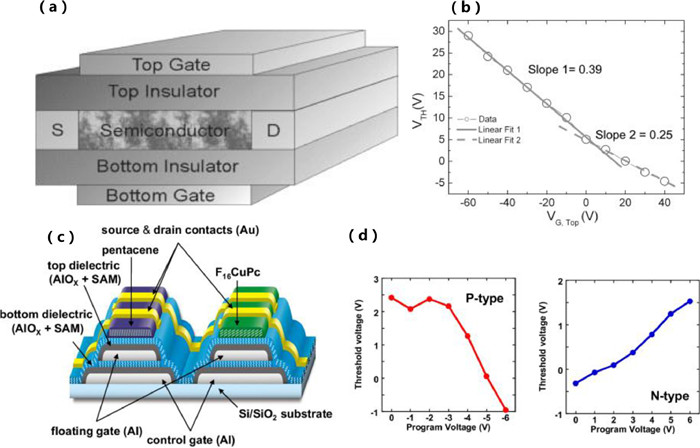
In addition to the approaches listed above, the adoption of innovative device architectures, such as dual-gate transistors and floating-gate transistors, is another appealing method for obtaining low threshold voltage OFETs. The device structures of typical dual-gate organic transistors and floating-gate organic transistors are given in Figs. 5a and c, respectively. In 2005, Cui and Liang prepared the first organic dual-gate transistor [68]. Dual-gate transistors feature greater currents, higher stability, and better channel controllability relative to traditional OFETs. Maddalena et al. demonstrated that the threshold voltage of the bottom gate is correlated with top gate bias in dual-gate transistors [69]. More specifically, there were two linear correlations between the top gate voltage and the bottom threshold voltage, which was caused by the contribution of the semiconductor layer's capacitance (Fig. 5b). Keeping the top gate voltage remained fixed. The total amount of charge generated by both gates can be expressed as Eq. 3.
|
|
(3) |
Among them, C1 represents the capacitance from the bottom gate to the channel, and C2 represents the capacitance from the top gate to the channel. When VGB reaches VTH, QG is equal to 0, and VTH can be described in Eq. 4.
|
|
(4) |
Taking p-type semiconductor as research object, the accumulation of charges occurs in the top channel when the top gate is negative. At this time, C1 = (1/CB + 1/CS)−1, C2 = CT, where CB, CT and CS are the capacitances of the bottom dielectric, top dielectric and semiconductor layer, respectively. By substituting this into Eq. 4, the value of k can obtain by Eq. 5. When the top gate is positive, the accumulation of charges occurs in the bottom channel. At this time C1 = CB, C2 = (1/CT + 1/CS)−1, the value of k can be expressed as Eq. 6.
|
|
(5) |
|
|
(6) |
When CS is large enough, the two slopes tend to be identical and equal to CT/CB, which is consistent with previous reports [70]. From the above analysis, we note that the threshold voltage can be precisely regulated when each capacitance value in the dual-gate transistor is determined.
Similar control over the threshold voltage has also been shown in floating-gate transistors by Someya's team [71]. Two gates are present in floating-gate transistors as well, but one of them is embedded within the dielectric layer. Through applying a sufficiently large program voltage in the control gate, the charge will enter the floating gate by quantum tunneling or thermal emission when the dielectric is thin enough. This charge on the floating gate will partially shield the electric field between the gate and the semiconductor, which thereby changed the threshold voltage. According to the above principles, this work could systematically adjust the threshold voltage of p-type semiconductor pentacene from 2.4 V to −1 V and n-type semiconductor F16CuPc from −0.3 V to 1.5 V (Fig. 5d).
Subthreshold swing is defined as the change of gate voltage required to change the channel current by one order of magnitude in the subthreshold operating region. The smaller SS means that the device can switch from OFF state to ON state more quickly. Similar to the threshold voltage, the smaller SS is beneficial to reduce the power dissipation of OFETs. Subthreshold swing can be expressed as Eq. 7.
|
|
(7) |
In this equation, kB is the Boltzmann constant, T is the temperature, q is the elementary charge. Thus, larger Ci and smaller Dit are advantageous for lowering SS. Furthermore, the minimum value of SS, that is, its theoretical limitation value at room temperature (T = 300 K) is 59.6 mV/dec.
Choi et al. synthesized a novel high-k ultrathin polymer dielectric by initiating chemical vapor deposition (iCVD) [72]. The 20-nm-thick polymer had a capacitance value as high as 270 nF/cm2. C8-BTBT transistors fabricated with this could achieve subthreshold swings as low as 98.5 mV/dec. Geiger and his coworkers used plasma-assisted oxidation to obtain ultrathin titanium oxide (TiOx) dielectric (Fig. 6a) [73]. The hybrid TiOx/self-assembled monolayer (SAM) dielectric showed a capacitance of 1.1 µF/cm2. And the SS of 2, 7-diphenyl[1]benzothieno[3, 2-b][1]benzothiophene (DPh-BTBT) OFETs was determined as 59 ± 1 mV/dec, which was not affected by channel length (Figs. 6b and c). It is worth mentioning that hydrophobic SAM in this work was beneficial to reduce the defect density on the interface, which also contributed to the ultra-low SS. However, the hydrophobicity of the dielectric will result in the inability to further reduce the defect density by growing organic semiconductor single crystals through solution method.

To solve the problem, Hasegawa's group developed a method called extended meniscus-guided (EMG) coating to grow phenyl/alkyl-substituted benzothieno[3, 2-b]naphtho[2, 3-b]thiophene (Ph-BTNT-Cn) single crystals on a highly hydrophobic dielectric [74]. Specifically, the authors deposited a U-shaped Au film on the surface of Cytop to initiate crystal growth and maintain the extension of the meniscus. In this way, the shape of the solution meniscus on the Cytop surface was consistent with the relatively hydrophilic Au surface, which facilitated the growth of single crystals. A schematic diagram of the mechanism of EMG coating is shown in Fig. 6d. Due to the effective elimination of charge traps at the interface, OFETs of Ph-BTNT-Cn single crystal achieved SS as low as 63 mV/dec, although the capacitance of the dielectric layer is only 23 nF/cm2. Apart from this unique solution-processed method, other strategies such as the flip-crystal technique [75], PVT or the "probe-assisted" method [76], microspacing in-air sublimation [77] are also proved to attain organic single crystal in the hydrophobic substrate and achieve a steep subthreshold swing.
Limited by the Boltzmann thermionic limit, how to further reduce SS to below 60 mV/dec is a great challenge. Recently, Wang and coworkers introduced ferroelectric hafnium oxides HZO with negative capacitance (NC) effect into OFETs based on 2, 9-didecyldinaphtho[2, 3-b: 2′, 3′-f]thieno[3, 2-b]thiophene (C10-DNTT) monolayer crystals [11]. The devices reduced the subthreshold swing to 56.5 mV/dec. Therefore, ferroelectric negative capacitor provided a solution for breaking the thermionic limit of SS.
The above-mentioned performance parameters of OFETs have complied with the basic requirements of their industrial production. However, as opposed to traditional FETs, the high contact resistance in OFETs leads to a series of problems, such as non-ideality of transfer characteristic curves and performance degradation caused by severe heat release. In particular, with the development of short-channel devices, the impact of contact resistance on performance become more severe as it accounts for a larger proportion of the total resistance [78-81]. Contact resistance in OFETs consists of injection resistance and bulk resistance. Injection resistance originates from the mismatch between Fermi levels of metal and HOMO levels (p-type) or LUMO levels (n-type) of organic semiconductors. Bulk resistance is associated with charge transport from the electrode-semiconductor interface to the channel. Therefore, low contact resistance can be achieved in terms of reducing both injection resistance and bulk resistance. To decrease the injection resistance, electrode interface modifiers like SAM and dopants are often used. Because of the large interface dipole to increase the metal work function, pentafluorobenzenethiol (PFBT) is the most commonly used SAM materials to enhance hole injection. Klauk's group used PFBT to modify Au as the bottom-contact electrode, and they demonstrated that contact resistances as small as 29 Ω cm could be obtained in 2, 9-diphenyl-dinaphtho[2, 3-b: 2′, 3′-f]thieno[3, 2-b]thiophene (DPh-DNTT) OFETs by further combining a sufficiently thin SAM/Al2O3 dielectric and optimized semiconductor layer thickness (Fig. 7a) [82]. It is worth mentioning that the difference of contact resistance between bottom-contact (BC) and top-contact (TC) OFETs was related to the gate dielectric thickness in this case (Fig. 7b). When the gate oxide was sufficiently small, contact resistance of BC OFETs was significantly smaller than TC OFETs, which was consistent with simulations in the literature [83,84]. Similarly, they obtained a contact resistance of 15 ± 5 Ω cm in the PFBT/Au (source and drain)-DPh-DNTT (semiconductor)-TiOx/SAM (dielectric) system [73].

Unlike the SAM layer, which changes the work function of the electrode, the dopant mainly increases the carrier concentration at the contact interface to reduce the width of the depletion region, so that carriers can be effectively injected by quantum tunneling [51]. Yamamura et al. obtained a contact resistance of 46.9 Ω cm by introducing the dopant 2, 3, 5, 6-tetrafluoro-7, 7, 8, 8-tetracyanoquinodimethane (F4-TCNQ) to the OFETs of 3, 11-dinonyldinaphtho[2, 3-d: 2′, 3′-d′]benzo[1, 2-b: 4, 5-b′]dithiophene (C9-DNBDT-NW) bilayer crystal [85]. Besides the commonly used F4-TCNQ [86,87], other dopants such as 1, 3, 4, 5, 7, 8-hexafluorotetracyanonaphthoquinodimethan (F6-TNAP) [88] and FeCl3 [89] were also used to reduce the injection resistance. In addition to the commonly used methods to reduce injection resistance, Stadlober and his colleagues formed a thin AuOx layer in the source and drain electrodes by UV/ozone treatment [90]. In this way, the morphology of pentacene at the interface was improved and the hole injection barrier was reduced. Hence, a small contact resistance value of 80 Ω cm was obtained.
It is not difficult to conclude from the above literature that reducing the bulk resistance is equally important with reducing the injection resistance. Obviously, the lower thickness and defect density of the organic semiconductor layer are favorable to reducing the bulk resistance. Thus, OFETs based on monolayer crystals have recently attracted great attention. However, the conventional vacuum deposition of source/drain electrodes will damage monolayer crystals and significantly impair the contact between the electrode and the semiconductor. As shown in Fig. 7c, Peng et al. demonstrated by cross-sectional transmission electron microscopy (TEM) that the vapor-deposited gold electrode would destroy the structure of organic crystals [91]. To solve this problem, they adopted the method called "gold electrode transfer", which was invented by Tang et al. [92]. By combining transferred Au contacts and the monolayer C10-DNTT crystal, the contact resistance could be as low as 40 Ω cm without the use of other complicated means (Fig. 7d). Furthermore, by shortening the carbon chains, the contact resistance can be further reduced. The contact resistance of C6-DNTT monolayer crystal is as low as 28 ± 3 Ω cm due to the decreased tunneling distance during carrier injection process [93].
Although low contact resistance of monolayer crystal OFETs have been achieved by electrode transfer method. However, this transfer method is only suitable for basic research due to its manual operation. Therefore, it is necessary to develop other non-destructive electrode preparation methods. Makita et al. peeled off the solution-processed electroless Au electrode and laminated them to monolayer C9-DNBDT-NW crystals [94]. This method could obtain patterned electrodes with a spatial resolution as low as 10 µm and avoid the destruction of organic semiconductors. Finally, they received a low contact resistance of 120 Ω cm.
With the continuous improvement of various performance parameters, OFETs are getting closer to practical applications. The stability, especially bias stress stability, has thus received great attention. Bias stress stability means that the device performance remains essentially unchanged when the OFET operate under continuous electrical bias. In contrast, bias stress instability is usually reflected in the changed source-drain current, decreased mobility, increased threshold voltage and subthreshold swing. Bias stress stability is very important for the application of OFETs. For instance, when organic light-emitting diodes (OLEDs) are driven by OFETs, higher threshold voltage may prevent the OLEDs from turning on normally, and changed source-drain current would affect the brightness of OLEDs. Although the cause of bias stress instability is still unclear, carrier trapping in OFETs is commonly acknowledged to be a contributing factor [12]. The trapping of carriers may come from three aspects, including trap states in the OFET, minority carrier injection and environmental factors.
In 2007, Batlogg's group combined rubrene and pentacene single crystals with hydrophobic dielectric Cytop to obtain OFETs with good bias stress stability [95]. They attributed this to two reasons: (1) The hydrophobic dielectric surface was substantially free of electroactive trap states; (2) Single crystals showed more ordered packing and fewer defect states. In 2013, they prepared various thin film included single crystal, thermally evaporated thin film and spin-coated thin film of n-type semiconductor N, N′-1H, 1H-perfluorobutyl dicyanoperylene carboxydiimide (PDIF-CN2) on Cytop, hexamethyldisilazane (HMDS) and SiO2 [96]. The results also proved that the single crystal on Cytop had the smallest density of trap states, showing optimum bias stress stability. Besides the commonly used polymer Cytop, another way to obtain hydrophobic surface is to modify the dielectric with SAM layers. Peng et al. transferred the evaporated C10-DNTT film to the SAM/AlOx dielectric including octadecylphosphonic acid (ODPA), phenylphosphonic acid (PhPA) and 1H, 1H, 2H, 2H-perfluorooctanephosphonic acid (FOPA) [97]. The experimental results showed that FOPA with the lowest surface energy, i.e., the best hydrophobicity, exhibited the best bias stress stability with less than 2% drain current change after 20, 000 s continuous bias. Similarly, a recent study by this group transferred C10-DNTT monolayer crystals to 1H, 1H, 2H, 2H-perfluorodecylphosphonic acid (FC10PA)/AlOx dielectric, which showed better bias stability than phenyltrichlorosilane (PTS)/SiO2 and ODPA/AlOx dielectric [98].
The topography control is equally crucial as the properties of the dielectric layers. Roh et al. found that the SAM layer with a shorter alkyl chain could cover more SiO2 surface, reduce more surface trap states and exhibit better bias stress stability. However, a longer SAM that could induce bigger grain size of pentacene was helpful to increase the mobility [99]. To overcome this tradeoff, this work proposed a two-step SAM-treatment, which treated long SAM and short SAM in sequence to ensure both the high mobility and good bias stress stability (Fig. 8a). Huang's group prepared a three-layer dielectric of PMMA/cross-linked poly(4-vinylphenol) (cPVP)/PMMA. The AFM images showed that the three-layer dielectric had the lowest roughness and pinhole-free morphology compared to the two-layer and single-layer dielectrics [100]. Therefore, the three-layer dielectric exhibited the best electrical insulating properties, and the grown pentacene had the smallest grain boundaries. Based on this, the IDS dropped by only 15% under the 1200 s operation while the single-layer and double-layer devices dropped by 80% and 90%. It is worth mentioning IDS of the three-layer device increased slightly in the initial 100 s, which could be attributed to the slow polarization of the hydroxyl groups in c-PVP.
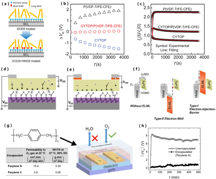
When bias is applied, the dipoles will align along the gate field and induce additional charge within the channel. This phenomenon is known as the polarization effect. Tang and coworkers took advantage of this effect by preparing a bilayer dielectric of relaxor ferroelectric polymer poly(vinylidene fluoridetrifluoroethylene-chlorofloroethylene) P(VDF-TrFE-CFE) and Cytop [101]. As shown in Figs. 8b and c, Vth and IDS of Cytop-based devices decreased under long-term biasing on account of trap states, while the P(VDF-TrFE-CFE)-based devices exhibited the opposite trend because of the polarization effect. Therefore, by combining these two dielectrics, the bias stress instability caused by the charge trapping and polarization effects could be canceled out. Similarly, Kippelen's group prepared gate dielectrics combined by Cytop and an Al2O3: HfO2 nanolaminate [13]. The threshold voltage almost keeps no change for periods of up to 5.9 × 10⁵ s. Analysis showed that two compensatory aging mechanisms led to this high stability, but the specific physical mechanism needs further study.
Furthermore, blending the semiconductor with insulating polymer is also a common method to improve the bias stress stability [102,103]. Campos et al. mixed the n-type semiconductor N, N′-bis(n-octyl)-dicyanoperylene-3, 4:9, 10-bis(dicarboximide) (PDI8-CN2) with polystyrene (PS). The performance parameters and bias stress stability were greatly improved [104]. They attributed it to a dual effect caused by phase separation. In detail, the bottom PS layer close to the dielectric layer reduced interfacial traps and the top thin PS layer with the self-encapsulation effect avoided the influence of water and oxygen. Other polymer insulator such as PMMA [105], high-density polyethylene (HDPE) [106], poly(pentafluorostyrene) (PFS) [107], are also used to improve the bias stress stability.
Along with reducing the inherent carrier trapping in OFETs, it is urgently necessary to prevent minority carrier injection, which will result in persistent carrier trapping and long-lasting bias stress instability. As shown in Fig. 8d, continuously injected electrons in a p-type device will neutralize the states occupied by holes and create new trap states for hole trapping, so the device will be in a state of long-term bias stress instability [108]. To avoid this situation, preventing minority carrier injection by means such as electrode modification or introduction of additives into the active layer is essential.
Increasing the minority carrier injection barrier by electrode modification is an effective means (Fig. 8e). In 2019, Zhou et al. inserted type-II electron-well materials molybdenum oxide (MoO3-x) between the electrode and the semiconductor. It could be seen from the Fig. 8f that MoO3-x took up electrons like an electron sink. Consequently, the electron injection into the active layer was prevented [109]. Experiments have shown that this method could improve the bias stress stability of various materials including organic semiconductors and graphene. However, in 2020, Yang et al. demonstrated that type-II electron-well materials might lead to doping of organic semiconductors, thereby affecting device performance [110]. Therefore, they proposed the use of type-I electron-injection-barrier materials with high LUMO levels. This class of materials could improve bias stress stability by increasing the electron injection barrier while not affecting other device performance. In particular, they also demonstrated that the electron injection efficiency decreased more with the higher energy offset between the LUMO level of the modified material and the Fermi level of the electrode. Similarly, Jie's group also demonstrated that the introduction of a wide-bandgap semiconductor (also with a high LUMO level) 2, 7-didecyl[1]benzothieno[3, 2-b][1]benzothiophene (C10-BTBT) could prevent electron injection and significantly improve bias stress stability [111].
In p-type devices, another simple method to suppress bias stress instability is adding electron acceptors to the semiconductor layer. Ford and his colleagues discovered that the introduction of electron acceptor [6,6]-phenyl-C61-butyric acid methyl ester (PC61BM) could convert bipolar transport of the conjugated polymer to p-type transport, which indicated that electron injection was suppressed [112]. After optimizing the experimental parameters, device performance showed no significant change even after 14.5 h of cycling. Further investigation showed that the added electron acceptor would trap injected electrons so that they would not lead to bias stress instability [113].
Although the bias stress stability of OFETs has been greatly improved, we note that in some of the summarized literature the OFET were tested in the glove box. This is mainly because environmental factors like water and oxygen can introduce new defects through various mechanisms such as reaction with charge carriers, the semiconductor degradation. Therefore, this problem needs to be solved to realize the practical application of OFETs.
Hydrophobic materials such as Cytop have been widely used to reduce the water-induced trap density, which has been mentioned above. In addition, reliable encapsulation layers are a more direct and effective means to isolate environmental factors. Recently, Jurchescu's group demonstrated that moisture, which created electronic traps, was responsible for the device performance degradation, while oxygen could improve performance through doping in devices based on p-type semiconductor tri(n-hexyl)silylethynyl benzodithiophene (TnHS BDT) trimer [114]. On the basis of this, they chose parylene N which had higher permeability to oxygen for encapsulation (Fig. 8g). They found the trap density of states (DOS) spectrum of the encapsulated device did not change within 500 min. Therefore, threshold voltage of the OFETs changed less than 1 V under 500 min bias as Fig. 8h showed.
After more than three decades of developments, OFETs have come a long way. The researchers increased the mobility from 10−5 cm2 V−1 s−1 to more than 20 cm2 V−1 s−1 through the synthesis of new materials, amelioration of processing methods and device interfaces, etc. In addition to this, other parameters such as threshold voltage and subthreshold swing have been paid attention. And the contact resistance has been reduced from the level of more than 100 kΩ cm to below 100 Ω cm. Further, through the majorization of materials and interfaces, as well as the development of encapsulation technology, the bias stress stability of the device is effectively improved.
Recent advances mentioned above have laid a solid foundation for application of OFETs. Actually, since organic FETs and inorganic FETs have different application scenarios, the better performance of OFETs is favorable but not all parameters must meet and exceed inorganic FETs. In light of the benefits of OFETs, future research should concentrate on the flexibility, integration, miniaturization, low power consumption, and high-frequency operation of the devices. And the above-mentioned five fundamental parameters are directly or indirectly related to these essential points for realizing the application of OFETs. For instance, miniaturization is related to contact resistance and low power consumption is related to SS and Vth. Researchers have made great progress in high-frequency OFETs [115,116], ring oscillators [117], skin electronics [118,119], high-density circuits [120], etc., in recent years, which indicates that the performance of OFETs has shifted from quantitative change to qualitative change. We look forward to further breakthroughs in circuits and flexible electronics of OFETs in the upcoming decade.
In addition to the fundamental applications, the advantages of OFETs are also manifested in multifunctionality due to the distinct optoelectronic properties, sensing properties and biocompatibility of organic semiconductor materials. The next section will review and prospect the recent progress in multifunctional OFETs.
OFETs are attractive candidates for electronic applications not only because their intrinsic flexibility, biocompatibility and solution processability, but also owing to their signal switching and transduction properties. Through molecule design and interface engineering, the conductive capability of conjugated semiconductors can be fine-tuned towards state-of-the-art multifunctional OFETs. In this section, we introduce the related progress in OFET-based sensors, OLETs, memory devices, artificial synapses and adaptive devices (Fig. 9). We expect that OFETs will be vital components in internet-of-things (IoT) and artificial intelligence (AI), including intelligent sensors, humanoid robotics, neuromorphic computing, display, optical communication, electrically pumped organic laser, etc.
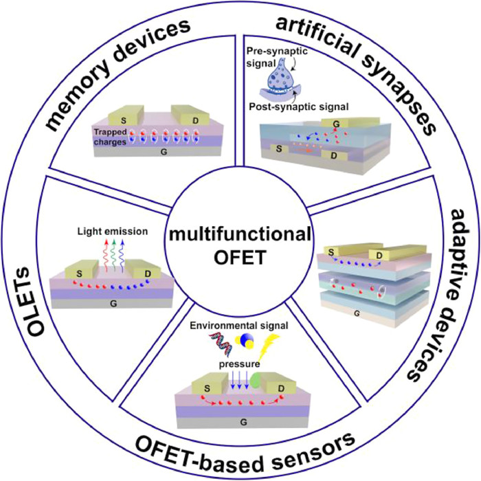
OFETs are capable of both signal switching and amplification. In terms of information processing, OFETs can meet the needs of different signal forms switching, device to device signal transmission and storage of external input signals. A typical OFET is three-terminal device in which the carrier concentration in the active layer can be effectively regulated by changing the gate voltage. This results in a regulation mode that combines a horizontal driving field and a vertical regulation field. In addition, the carrier concentration and mobility can be fine-tuned by other external fields and stimuli, thus giving the OFETs a variety of functionality. The so-called multifunctional OFETs generally show well-regulated current outputs on combined fields, such as sensors, memory devices, artificial synapses and novel adaptive devices, either show multiple signal outputs on a typical field modulation. For example, organic light-emitting transistors output both light and electrical signals, which is a perfect way of combining the switching properties of OFET with the emission properties of organic light-emitting diode [19]. Nonetheless, different OFETs have many commonalities in physical mechanism, interface engineering and device configuration (expect OLETs here). One is to form direct interactions between semiconductors and stimulus. The performance of devices can be quantitatively determined by the combined field of the gate voltage and the exposed stimulus, such as carrier concentration and mobility. Following this way, multiply OFET-based sensors can enable detection of various biological species and physical signals (including pressure, temperature, light, etc.) [121,122]. The other way to fabricate multifunctional OFETs relies on manipulation carrier concentrations by modulating gating fields coupled with external stimuli. The carrier concentration in OFETs is decided by the gate voltage, the interface the trap density of the interface between semiconductor and dielectric layer and the capacitance of the dielectric layer, so it is essential to construct devices with designed the interfaces of dielectric/organic layer. In this section, we attempt to present a brief overview of recent advances and perspectives about multifunctional OFETs.
Sensors have become a necessary part of intelligent perception system. Different types of sensors have been widely used in different fields such as odor sensing, food monitoring, pathogen detection and medical diagnosis. When ambient signals are introduced, output in-situ can be converted and amplified electrical signal by the physicochemical interaction between the stimulus signal and the functional layer. A classical sensing process is described as follows. When the device is placed in an environment with detectable substances, non-covalent bonds (such as hydrogen bonds and π-π interactions) generate more attraction between the detectable substances and the functional molecules of the devices. The interaction leads to changes in carrier density and/or carrier transport properties in the conductive channel and results in changes in device characteristics. In 1990, Inganäs et al. found that the mobility and conductivity of poly(3-hexylthiophene) (P3HT) thin film devices decreased when exposed to ammonia (NH3), and the signal response was related to the film thickness, which lays a foundation for the development of OFET-based sensors [123]. And then, it has been developed that a series of regulation strategies of the sensor performance, including the introduction of specific functional groups in conjugated framework or side chain by molecular synthesis, the deposition or in-situ modification of receptor functional layer, the preparation of ultra-thin and porous organic semiconductor films, the design of dielectric layer and gate with micro/nano structure and the construction of organic electrochemical transistors by combining electrochemical principles. A series of highly sensitive physical signals, chemical gasses and biosensors have been developed to successfully achieve specific and sensitive detection of pressure, temperature, gas, ions, proteins, nucleic acids, drug molecules, etc. (Fig. 10a).
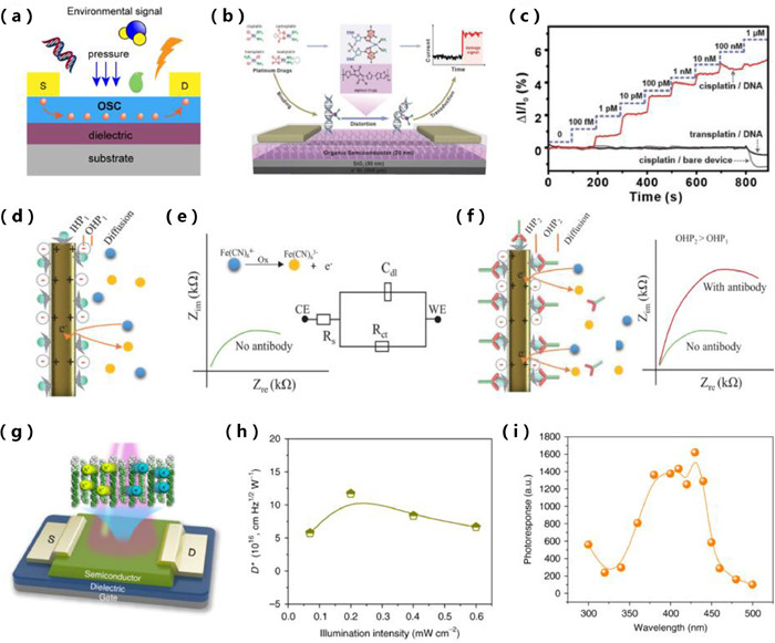
Since 2020, the important development trend of OFET-based sensors is to realize the detection of complex signals or signals in complex environments, especially fast and ultra-sensitive sensing of biological substances. Zhu's group reported an ultra-sensitive DNA damage detection sensor based on OFET device structure [16]. By combining the semiconductor interface with the DNA configuration change of platinum drug response, the charge distribution regulation and efficient signal amplification at the transistor interface (Figs. 10b and c). It was achieved within 20.5 s that the detection of DNA damage induced by 1 pmol/L cisplatin. Furthermore, a biochip that can be used for intelligent damage analysis in complex environments is designed, which provides potential for high-throughput biotoxicity evaluation and drug screening in the future. In addition to the new sensing principle, people continue to combine the advantages of organic electrochemical transistor (OECT) such as low voltage and high transconductance to explore the specific detection of biomolecules in complex environments. For example, Rahul's group proposed an advanced nanomaterial-based biosensing platform that detects COVID-19 antibodies within seconds [124]. The device is fabricated by creating a gold microcolumn array electrodes using Aerosol Jet nanoparticle 3D printing method, and then functionalizing the reduced-graphene-oxide (rGO) nanosheets using a coupling chemistry of 1-ethyl-3-(3-dimethyl-aminopropyl)carbodiimide, N‑hydroxy-succinimide (EDC: NHS) chemistry and immobilizing antigens on the electrode surface. Antibodies are detected by electrochemical transduction when antibodies in the introduced fluid form immune complexes with antigens on the surface of the 3D electrode (Figs. 10d–f). The sensor can be regenerated within a minute, allowing continuous detection of samples using the same sensor. And the device has excellent specificity and ultra-low detection limit. Recent results show that OFET can also be used for ultra-sensitive pressure and light detection [125].
In addition, a lot of progress show that OFETs can also be used for ultrasensitive pressure and light detection [126-129]. Especially in the aspect of photodetection, a series of organic phototransistors (OPTs) have been developed by combining the energy bandgap modulation of conjugated molecular and the optimization of device structure [125]. In 2019, Hu et al. successfully developed band-like transport in small-molecule thin films for high mobility and ultrahigh detectivity phototransistor arrays with vacuum-deposited 2, 6-diphenylanthracene (DPA) as organic photo-responsive layers (Figs. 10g–i) [130]. The low mobility of most photosensitive materials limits the carrier transport and collection efficiency. Some single-crystal phototransistors show excellent mobility and photo-sensitivity; however, it is a challenge for large-scale fabrication and applications that precise control of single crystal growth. In this case, small-molecule thin-film field-effect transistors based on vacuum-deposited DPA exhibit band-like transport, which means that the films are highly crystalline. It can be operated at very low dark currents (~10−12 A) with a detectivity greater than 1017 cm Hz1/2 W−1.
Organic light-emitting transistor is a miniaturized optoelectronic integrated device that combines two device functions of OFET and organic light-emitting diode (OLED) in the same device. On the one hand, it has the switching and signal amplification functions of OFETs [131]. On the other hand, it has the electroluminescent characteristic of OLEDs, therefore, it has important research significance in the research of basic properties of organic materials, new flexible display/lighting, organic electrically-pumped lasers, and integrated optoelectronic devices [132]. Thus, it offers great promise for reducing the complexity of the process of next-generation pixel circuits. In OLETs, the electrical switching is regulated by the current between the drain and source at the gate bias voltage, while electroluminescence (EL) occurs due to the electron-hole recombination in the transistor channel (Fig. 11a) [133]. Excitons are generated by the recombination of in-plane electron and hole current during device operation, which are adjusted by the gate electrodes. Therefore, OLET with three-electrode device structure is considered as an excellent platform for researching the basic physical processes of charge injection, charge transport, charge carrier recombination and electroluminescence in organic semiconductor devices [134-136]. In 2003, Hepp et al. proposed the first conceptual OLET devices, which has received significant attention and research from academia and industry [137]. Zaumseil et al. reported the OC1C10-PPV-based bipolar light-emitting transistors with a BCB buffer layer, which has effective electron and hole carrier transport and good excellent photoluminescence efficiency in 2006 [138]. Electrons and holes injected from separate calcium and gold electrodes are recombined in a radiative manner within the channel in this device. The composite region with applied gate and source-drain bias can be moved to any site in the channel. It is demonstrated a direct visualization and demonstration of the coexistence of electron and hole accumulation layers in a bipolar transport regime.

The application of organic semiconductor materials with both high mobility and high luminescence properties is crucial for the construction of high-performance OLETs. The former determines the electrical switching capability of the OLETs, while the latter directly determines the optical output performance. However, high mobility and strong luminescence properties are a pair of contradictions from the perspective of molecular design, and it is difficult to achieve effective integration of the two aspects in the same molecular system. Therefore, the development of high-mobility light-emitting/laser organic semiconductor materials has always been a challenging problem in the field of organic electronics. To some extent, it also limits the research on high-performance OLETs and related applications. In 2021, Yu's group illustrated a synergy between photoluminescence and charge transport achieved by finely tuning polymeric backbones for OLETs (Figs. 11b and c) [139]. Semi-ladder polymers with luminescent and charge transport properties were prepared by the copolymerization of weak acceptors (TPTQ or TPTI) and weak donors (fluorene (F) or carbazole (C)). It was found that the delicate balance of high crystallinity, heighted planarity, and interchain aggregation obtained in the copolymer TPTQ-F promotes high ambipolar charge mobility and photoluminescence quantum yield. TPTQ-F exhibits an external quantum efficiency (EQE) of 5.3% in the multilayered OLETs.
The most direct application field of area emission OLETs is panel display devices. Compared with active-matrix OLED (active-matrix organic light-emitting diode, AMOLED) display devices, this highly integrated structure can not only achieve higher resolution, but also can be fabricated by lower-cost technologies such as roll-to-roll. However, the great challenge of achieving uniform regional emission in OLET with good stability and arbitrary tunability has hindered their development in this field. In 2021, Hu et al. constructed RGB OLETs with uniform area emission (Figs. 11d and e) [132]. By incorporating a charge transport buffer (CTB) layer between the conductive channel and the emitter layer, the potential under the drain is redistributed under the shielding effect of the CBT layer, resulting in a highly uniform current density. It is crucial for the formation of area emission in OLETs that uniform recombination of balanced holes and electrons can be guaranteed. The RGB OLETs exhibited high ON/OFF ratio up to 106, good stability over 200 cycles and high aperture ratio over 80%. Due to the arbitrary tunability of the device geometry and good compatibility with traditional fabrication techniques, it has great potential in display technology.
Organic laser emission has always been an important research field. In traditional OLEDs, the current density is low and laser emission cannot be achieved due to low charge mobility of the active materials. OLETs provide a way to obtain high current density, but due to the presence of grain boundaries in the thin film devices, the mobility is too low to give organic lasers. Thinking of the OFET, organic single crystals have far fewer boundaries and higher mobility than the thin films [140]. This illustrates that the use of organic single crystals is a possible route to realize organic lasers emission. In 2021, Hu's group reported a high-mobility organic laser semiconductor 2, 7-diphenyl-9H-fluorene (LD-1) (Fig. 11f), which exhibits excellent crystalline-enhanced emission by carefully tuning its crystal growth process (Fig. 11g) [141]. The one-dimensional LD-1 nanowires have high absolute photoluminescence quantum yield (PLQY) up to 80%, high charge carrier mobility about 0.08 cm2 V−1 s−1 and excellent FP lasing characters (Fig. 11h). It is of great significance to carry out research on organic electrically pumped lasers and other integrated electrically driven photonic devices.
With the progress of science and technology and the development of economy, our society has entered the era of big data, 5G, AI, IoT, etc. Memory semiconductor market began a new round of explosive growth. The memory based on organic semiconductor has many advantages, such as low cost, simple structure, large-area processing, flexibility. The most important point is that the molecular size of organic semiconductor materials is 1–100 nm, so memory devices based on organic semiconductor molecules are expected to obtain nanometer-sized memory cells, which can greatly improve the storage density and reduce the size of memory devices. Three-terminal OFET memory has many advantages compared to two-terminal device. For example, accurate charge modulation, non-destructive readout, ease of integration and multi-bit storage. The structure of the OFET-based memories is based on the organic field effect transistor structure, the main difference is that the memory of the transistor structure has an additional charge trapping layer. However, conventional OFETs have no the function of the storge. In general, memory requires at least two different states to represent the "0" and "1" as binary information. As for OFET-based memory, storge states are encoded by modulating carrier trapped states on the dielectric layer or the interface between the gate dielectric and the organic layer, which is represented by offsets in threshold voltage. And it has the flexible ability to switch between two states. According to the structure and the principle of the charge storage, OFET-based memory can be divided into floating-gate memory, polymer electret memory, ferroelectric memory and other types of memory (Fig. 12a). The first floating-gate memory was reported by Kahng and Sze in 1967 [142]. When performing a "programming" or "erasing" operation, electrons or holes are directly trapped or released by the floating gate layer or Fowler-Nordheim tunneling. The vertical electric field of the devices between the gate and the channel can shielded by the trapped charges, which gives rise to an offset of the threshold voltage. Above all, the gate voltage can effectively regulate the amount of charge on the floating gate. In 2018, Jaeyoung et al. presented a novel CdSe quantum-dot floating gate memory that can be erased using light bias (Fig. 12b) [143]. This work introduced three different organic molecules on the surface of CdSe quantum dots as photo-floating gate layers, resulting in efficient hole diffusion from the CdSe quantum dots to the conductive channel. More interestingly, light-induced recovery results in faster erasing process. This memory exhibits high ON/OFF ratios > 105 over 10000 s, and excellent switching endurance within 1 s through both voltage-driven programming processes and light-assisted erasing processes (Fig. 12c).

Similar to floating gate OFET-based memories, the operation mechanism of the polymer electret OFET-based memory is also charge trapped. With an applied electric field, the polarization phenomenon will not completely disappear due to the removal of the applied electric field in some dielectrics. Instead, polarization charges will "permanently" exist in the interior and surface of the dielectric, which called electrets. In other word, electrets are dielectric materials with quasi-permanent charge or dipolar polarization. Recently, Huang et al. designed a high-performance nonvolatile organic field-effect transistor memory based on organic semiconductor heterostructures of pentacene/P13/pentacene as both charge transport and trapping layers (Fig. 12d) [144]. The discrete n-type P13 implanted in the p-type pentacene layer, which cannot only facilitate the electron capture process, the pentacene/P13/pentacene-like quantum well organic heterostructure can also act as a charge trapping sites. The charge trapping properties of the poly(4-vinylphenol) (PVP) layer and the charge trapping of discrete P13 collectively enhance the memory performance (Figs. 12e and f). Besides, trilayer organic heterostructures can also be widely applied in multilayer flexible non-volatile memory devices in the future.
Ferroelectric phenomenon refers to the spontaneous polarization of ferroelectric materials when there is no external electric field. The gate insulator in ferroelectric memory is made of ferroelectric material. The polarization state of the ferroelectric insulator is changed by applying an external force voltage, thereby accurately adjusting the carrier concentration in the channel. It has been widely used in storage field because of the advantages of nondestructive read, fast operation speed and low power consumption. Recently, Paolo et al. proposed multi-responsive nonvolatile memories based on optically switchable ferroelectric OFETs (Fig. 12g) [21]. This work uses a ferroelectric gate insulator layer combined with optically switchable molecules implanted in a semiconducting polymer matrix. Different stimuli cause the memory element to switch between different memory states: light or electric fields, leading to two independent ways of programming or erasing processes (Fig. 12h). The device can easily and directly switch between multiple current levels, accurately control the readout signal and have outstanding repeatability and endurance. In addition, it was demonstrated that the capability of relatively faster and lower optical power intensity optical write operations of memory states while maintaining a high readout signal-to-noise ratio.
In biological nervous systems, synapses act as the perception and processing units required for signal transmission between neurons [145]. The synaptic structure of the organism includes the presynaptic membrane, the synaptic cleft and the postsynaptic membrane. The presynaptic membrane releases neurotransmitters in the synaptic cleft, and the postsynaptic membrane receives neurotransmitters, changes the resting potential, and completes the conduction of electrical impulses between neurons. According to the difference of electrical signals in the response of the postsynaptic neuron, it can be divided into excitatory postsynaptic current (EPSC) and inhibitory postsynaptic current (IPSC), which is generated by the release of exciting or inhibiting neurotransmitters under external activation, that then facilitate or depress signal transmission in the synapses, respectively. The strength of connections between pre- and post-neurons is defined as synaptic weights, and studies of changes in weights are collectively referred to as synaptic plasticity, which underlies the function of learning and memory [146]. According to the changes of synaptic weight, it can be generally classified into short-term plasticity (STP) and long-term plasticity (LTP), time-dependent synaptic plasticity (STDP) and so on. These effects have been defined as facilitation and depression, which are reflected by the corresponding postsynaptic currents. In artificial neural networks, electronic devices are an important part of the synapses to emulate the operation of the brain. The gate, insulating layer and active layer of OFET correspond to the presynaptic membrane, the synaptic cleft and the postsynaptic membrane in function, which can be used as an effective carrier to simulate synapses.
Considerable research efforts have been devoted to the development of artificial synapses, Alibart et al. introduced gold nanoparticles into the semiconductor layers of pentacene and simulated STP and other synaptic behaviors using the dynamic storage and release of nanoparticles [147]. Malliaras et al. reported the synaptic transistor based on poly(3, 4-ethylenedioxythiophene): poly(styrene sulfonate) (PEDOT: PSS), and a series of synaptic devices based on electrolyte insulation layer OFET and OECT have been developed successively [145,146]. These devices exhibit excellent low-voltage operation, non-volatile and low power consumption, and successfully simulate a series of the functions, such as STP, LTP and polymorphic storage in neural system.
In addition to the electrical and optical stimuli that have been extensively explored in recent years, the other stimuli (such as magnetic, tactile and thermal) also deserve attention because they have been studied only slightly and can contribute to a more thorough comprehension of neuromorphic systems [148-152]. These stimuli can induce switching of the synaptic devices between bistable or multi-stable states. It has shown that the application of electric fields can trigger ion migration, electron/hole transfer, phase changes, magnetic domain wall motion and ferroelectric polarization, while light illumination can induce carrier transport and chemical reactions. Among the other stimuli, both magnetoelectric coupling and pressure-electricity conduction depend on the properties of the materials involved, and resistive heating occurs in all electronic devices. The single transistor, however, struggles to simulate more advanced biological functions. Further, researchers have integrated synaptic transistors with devices owing different functions to construct artificial perception systems that can be used to artificial afferent nerves, reflex arcs, and learning and memory systems [148,153].
For example, Lee et al. presented and experimentally demonstrated an organic synaptic transistor with ferroelectric nanocomposite gate dielectric of barium titanate nanoparticles and poly(vinylidene fluoride-trifluoroethylene) (AiS-TSO) inspired by human "Michael's cells", which simulates the synaptic plasticity of Michael's cells (Figs. 13a and b) [22]. Based on the triboelectric-capacitive coupling effect, tactile stimulation can change the polarization state of the ferroelectric insulating layer, achieving controllable modulation of the carrier concentration at the conducting channel. Modulation of synaptic weight by varying the nanocomposite composition of gate dielectric layer enabled tuning of filtering and sensory memory functions (Figs. 13c and d). The device can not only quantitatively respond to external tactile stimuli (including external force intensity, frequency, time, etc.), but also simulate the memory function of sensory system by constructing flexible arrays, which is expected to be applied in the field of tactile perception (Figs. 13e and f). Alberto et al. reported a low-voltage artificial synapse made with inexpensive and commercially available plastic materials for neuromorphic computing (Figs. 13g and h) [145]. Interestingly, the paired pulse facilitation demonstrated two characteristic timescales, τ1 = 14 ms, τ2 = 240 ms, approximately equal to those measured in biological synapses. It has been determined that the artificial synaptic switch has a low energy density, and illustrate that only 35 aJ is sufficient to switch submicron devices, a number smaller than that of biological synapses. The artificial synapses are also fabricated on flexible substrates enabling the integration of neuromorphic functionality in stretchable electronic systems, which open a path towards extreme interconnectivity comparable to the human brain (Fig. 13i). These advances strongly demonstrate the important application prospect of OFET-based artificial synapses in the field of building sensory devices.

Driving by rapid development of AI, a series of smart devices have been developed that can mimic or even exceed human perception capabilities [154-156]. As one of the most vital functionalities of biological systems, adaptation can enable dynamic fitness to varying environmental conditions, which enables weak sensory input to be amplified and prevents saturated to strong stimuli. External stimulus signals can be converted into limited neural signals for information processing and compilation through adaptation. The front end of the human peripheral nervous system contains a variety of sensory receptors such as vision, smell, touch, taste [157]. All receptors can complete the process of adaptation by adjusting their own electrical signal output to respond to changes in external environmental stimuli. In the case of human photoreceptors, the incident light intensity on the retina differs by ten orders of magnitude from day to night. However, the range of the optic nerve signal is no more than two orders of magnitude [158]. The human eye must adjust its visual sensitivity at any time according to the stimulus of different intensities of external light, and this dynamic adjustment process relies on visual adaptation. Adaptive devices, which aims to adjust the electrical signal behaviors dynamically according to external environmental changes to simulate the perception capabilities of living organisms, with dynamic modulation and information pre-processing capabilities, are attractive candidates for new generation of perception devices [159]. However, recreating sensory adaptation in solid-state devices is still in its infancy considering the complex requirements of fine-tuning electric signal by modulating electric field coupled with external stimuli. Previous efforts in mimicking sensory adaptation have been developed since 1990s based on complementary metal-oxide-semiconductor (CMOS) circuits, leading to complicated logic design and inefficient power consumption. Recently, much attention has been concentrated in constructing adaptive elements within a single device, which boost the rapid development of this emerging area.
Mimicking sensory adaptation within an OFET remains a daunting task due to the contradictory requirements of short-term decay and long-term stability of electrical signal in the same conductive channel. In 2019, Zhu's group firstly developed an organic adaptive transistor (OAT) by introducing PVA/poly[2, 5-bis(3-tetradecylthiophen-2-yl)thieno[3, 2-b]thiophene] (PBTTT) dynamic-trapping interface within the dielectric layer (Fig. 14a) [160]. The device exhibits rapid response, adaptive decay behavior, as well as long-term stable and cyclic operation under the stimulation of continuous gate voltage (Fig. 14b). The decay time constant is controllably adjusted between 50 ms and 5 s, which is consistent with various adaptive receptors in living body. Furthermore, integrating the OAT device and the pressure sensor can mimic the haptic adaptation behavior of the human beings. It has been successfully realized the dynamic simulation and function display of the slow and fast adaptation process of the OAT device to external pressure stimuli through the construction of integrated circuits and LED driver display (Fig. 14c).

Based on the achievements above, an advanced goal of adaptive OFETs relies on the achievements to enable autonomous response to varying external stimuli. Inspired by two different ion-gating phototransduction process in photoreceptors, Zhu's group created a light intensity dependent organic active adaptation transistor (OAAT) that consists of two complementary bulk heterojunctions (BHJs) in 2021 (Fig. 14d) [23]. The two BHJs initiate a photovoltaic effect-induced photoexcitation, as well as dynamic charge trapping-dominated inhibition, which couple together to modulate carrier concentration in the conductive channel. The device exhibits dynamic adaptation behavior for light intensities ranging over six orders of magnitude (1 ~ 1 × 10⁶ cd/m2), which fully covered the daytime conditions. And such a device can be classified into three distinctive models: from an ultraslow-adaptation (τ > 100 s) to slow adaptation (1 < τ < 100 s) and fast-adaptation (τ < 1 s) (Figs. 14e and f). They also proposed an active adaptation index (AAI) as a standard performance metric to quantitively evaluate the adaptation performance, which defines as the change in time-dependent photosensitivity as a function of orders of magnitude changes of luminance (dPt/dlogL). This tendency is consistent with the AAI adaptation rule extracted from the human visual system, suggesting the successful realization of bionic visual adaptation with the fabricated device. More importantly, the time-dependent AAI working model of the device is established through systematic mechanism research, which lays the foundation for the rational design of OAAT. In addition, the flexible device array (3 × 3) exhibits fast adaptation speed of less than 2 s under 1 × 10⁴ cd/m2, which is superior to the human eyes and that further verifies the advanced visual adaptation capabilities of OAAT. This result paves a new way for the construction of artificial visual perception system, which can potentially serve as a promising system for encoding dynamic stimuli and use in the robotics and biomimetic visual prosthetics. However, the reported adaptive devices are still in the beginning stages of mimicking adaptation behaviors individually, mainly based on tactile- and visual-adaptation devices [161]. Much efforts should be devoted to multi-mode perception adaptation devices in the future. An important direction is developing multi-mode perception adaptation mechanisms in the future.
With rapid development of OFETs in the past few years, multifunctional OFETs have drawn great attention but still remain greatly challenging. With the significant increase in sensitivity and selectivity of OFETs, many issues remain to be resolved, the devices should take possession of excellent stability, uniformity, repeatability and electronic neural interfaces with full challenge. Moreover, large-scale, light weight and high-density devices are also an important development trend in the future. To seize new chances for multifunctional OFETs, it remains a challenge to balance the electrical and mechanical properties of organic transistors. The future multifunctional OFETs should be flexible and implantable, which play an important role in various areas such as rollable displays, bendable smart cards, flexible sensors and remote diagnosis. With the rise of intelligent matter, an exciting topic is to develop smarter perception systems, which requires the integration of various multifunctional devices. For example, sensors, artificial synapse, adaptive devices, oscillators and other devices should be integrated to enable the next generation artificial systems. As one ideal route, complex functions should be based on a single device in order to peruse the simplest geometry and design complexity.
In short, the multifunctional OFETs have made great achievements, but there is still a long way to go. Further development should focus on the research of multifunctional materials, the optimal design of device structures and the in-depth understanding of its intrinsic mechanism and integration of the devices. With continued systematic research on these challenges, multifunctional OFETs are expected to provide new opportunities for organic electronics and make a great impact on various fields.
Over the past few decades, explosive progress has been achieved in the area of OFETs, from high-performance OFETs to multifunctional OFETs. In this review, we are committed to provide overall advancement in this emerging field around effective protocols for improving the performance parameters of OFETs and the burgeoning multifunctional OFETs. Briefly, since various device performance indicators have essentially satisfied the needs, the development of OFETs is progressing from the initially basic material and device research to the development of integrated circuits and functional devices.
Despite the remarkable advances achieved in high-performance OFETs and multifunctional OFETs, the research on OFETs gradually slow down and OFETs have not made any ground-breaking commercial applications yet. To realize the potential applications of OFETs in daily life, some existing problems and new challenges should be addressed: (1) High-performance n-type semiconductors and ambipolar semiconductors are urgently needed for integrated circuits. We note that there has been some research in this area [162-166], but it still suffers from low solubility, instability in air, non-ideal electrical characteristics and unbalanced electron/hole mobility, etc. (2) The contact resistance of OFETs is still much higher than inorganic transistors though some recent reports have reduced the contact resistance below 100 Ω cm. Further reducing the contact resistance to below 1 Ω cm is very meaningful for high-density device integration. (3) Similar to silicon-based transistors, doping technologies is fundamentally important for the future development of efficient and reliable organic electronics. Therefore, development of mature organic semiconductor dopants, doping technology and doping theory are necessary. (4) To achieve application in daily life, large-area uniformity and long-term stability of the device need to be further improved. (5) Structure-property relationship [167,168], sources of bias stress instability [169] and device interface issues [170] still require further in-depth research. (6) Most of the multifunctional OFETs are still at the proof-of-concept prototype stage, and it is necessary to deeply study the intrinsic mechanism of multifunctional OFETs and further advance the various properties to facilitate their commercial applications. (7) Taking into account the advantages of organic materials, multifunctional OFETs still require further improving the biocompatibility, flexibility and other characteristics by new material synthesis and better design of device structures, etc. Overall, OFETs show promising potential towards practical applications. Future research on OFETs needs continuous investment of intelligence and effort. We hope that this review will pave a way to boost further study of OFETs.
The authors declare that they have no known competing financial interests or personal relationships that could have appeared to influence the work reported in this paper.
This work was supported by the National Key Research and Development Program of China (Nos. 2019YFE0116700 and 2019YFA0705900), Ministry of Science and Technology, National Natural Science Foundation of China (Nos. 62075224, 22021002, 51873182 and 52103231), Zhejiang Province Science and Technology Plan (No. 2021C04012), and Zhejiang Provincial Department of Science and Technology. This work was also supported by the Lu Jiaxi International Teams Project (No. GJTD-2020–02) and the Fundamental Research Funds for the Central Universities (No. 2021QNA4033).
M. Saravanan, E. Parthasarathy, Microelectron. J. 114 (2021) 105102. doi: 10.1016/j.mejo.2021.105102
C. Dai, Y. Liu, D. Wei, Chem. Rev. 122 (2022) 10319–10392. doi: 10.1021/acs.chemrev.1c00924
X. Yao, Y. Zhang, W. Jin, Y. Hu, Y. Cui, Sensors 21 (2021) 995. doi: 10.3390/s21030995
M.D. Bishop, G. Hills, T. Srimani, et al., Nat. Electron. 3 (2020) 492–501. doi: 10.1038/s41928-020-0419-7
K. Sim, Z. Rao, Z. Zou, et al., Sci. Adv. 5 (2019) eaav9653. doi: 10.1126/sciadv.aav9653
Y.S. Rim, J. Inf. Disp. 21 (2020) 203–210. doi: 10.1080/15980316.2020.1714762
A. Tsumura, H. Koezuka, T. Ando, Appl. Phys. Lett. 49 (1986) 1210–1212. doi: 10.1063/1.97417
Y. Yuan, G. Giri, A.L. Ayzner, et al., Nat. Commun. 5 (2014) 3005. doi: 10.1038/ncomms4005
M. Chu, J.X. Fan, S. Yang, et al., Adv. Mater. 30 (2018) 1803467. doi: 10.1002/adma.201803467
P. Hu, X. He, H. Jiang, InfoMat. 3 (2021) 613–630. doi: 10.1002/inf2.12188
Z. Luo, B. Peng, J. Zeng, et al., Nat. Commun. 12 (2021) 1928. doi: 10.37188/cjl.20210304
S. Park, S.H. Kim, H.H. Choi, B. Kang, K. Cho, Adv. Funct. Mater. 30 (2019) 1904590.
X. Jia, C. Fuentes-Hernandez, C.Y. Wang, Y. Park, B. Kippelen, Sci. Adv. 4 (2018) eaao1705. doi: 10.1126/sciadv.aao1705
C.A. Di, F. Zhang, D. Zhu, Adv. Mater. 25 (2013) 313–330. doi: 10.1002/adma.201201502
C.A. Di, H. Shen, F. Zhang, D. Zhu, Acc. Chem. Res. 52 (2019) 1113–1124. doi: 10.1021/acs.accounts.9b00031
D. Ye, J. Wang, H. Shen, et al., Adv. Mater. 33 (2021) 2100489. doi: 10.1002/adma.202100489
X. Jiang, C. Sun, C. Zhang, S. Cheng, Chin. Chem. Lett. 32 (2021) 3364–3367. doi: 10.1016/j.cclet.2021.04.005
Y. Wu, X. Wang, X. Li, Y. Xiao, Y. Wang, Chin. Chem. Lett. 31 (2020) 99–102. doi: 10.1016/j.cclet.2019.04.074
C.F. Liu, X. Liu, W.Y. Lai, W. Huang, Adv. Mater. 30 (2018) 1802466. doi: 10.1002/adma.201802466
Z. Qin, C. Gao, H. Gao, et al., Sci. Adv. 8 (2022) eabp8775. doi: 10.1126/sciadv.abp8775
M. Carroli, A.G. Dixon, M. Herder, et al., Adv. Mater. 33 (2021) 2007965. doi: 10.1002/adma.202007965
Y.R. Lee, T.Q. Trung, B.U. Hwang, N.E. Lee, Nat. Commun. 11 (2020) 2753. doi: 10.1038/s41467-020-16606-w
Z. He, H. Shen, D. Ye, et al., Nat. Electron. 4 (2021) 522–529. doi: 10.1038/s41928-021-00615-8
H. Dong, X. Fu, J. Liu, Z. Wang, W. Hu, Adv. Mater. 25 (2013) 6158–6183. doi: 10.1002/adma.201302514
C. Wang, H. Dong, W. Hu, Y. Liu, D. Zhu, Chem. Rev. 112 (2012) 2208–2267. doi: 10.1021/cr100380z
J. Ren, X. Shu, Y. Wang, et al., Chin. Chem. Lett. 33 (2022) 1650–1658. doi: 10.1016/j.cclet.2021.10.052
Q. Wen, Q. Cai, P. Fu, et al., Chin. Chem. Lett. 34 (2023) 107592. doi: 10.1016/j.cclet.2022.06.015
H. Jiang, W. Hu, Angew. Chem. Int. Ed. 59 (2020) 1408–1428. doi: 10.1002/anie.201814439
C. Wang, H. Dong, L. Jiang, W. Hu, Chem. Soc. Rev. 47 (2018) 422–500. doi: 10.1039/c7cs00490g
Y.G. Zhen, H.L. Dong, L. Jiang, W.P. Hu, Chin. Chem. Lett. 27 (2016) 1330–1338. doi: 10.1016/j.cclet.2016.06.023
S. Riera-Galindo, A. Tamayo, M. Mas-Torrent, ACS Omega 3 (2018) 2329–2339. doi: 10.1021/acsomega.8b00043
Z. Zhang, L. Jiang, C. Cheng, et al., Angew. Chem. Int. Ed. 55 (2016) 5206–5209. doi: 10.1002/anie.201601065
P. He, Z. Tu, G. Zhao, et al., Adv. Mater. 27 (2015) 825–830. doi: 10.1002/adma.201404806
T. He, M. Stolte, C. Burschka, et al., Nat. Commun. 6 (2015) 5954. doi: 10.1038/ncomms6954
D. Liu, X. Xiao, Z. He, et al., Sci. China Chem. 63 (2020) 1221–1229. doi: 10.1007/s11426-020-9793-2
M. Li, A.H. Balawi, P.J. Leenaers, et al., Nat. Commun. 10 (2019) 2867. doi: 10.1038/s41467-019-10519-z
G. Giri, E. Verploegen, S.C. Mannsfeld, et al., Nature 480 (2011) 504–508. doi: 10.1038/nature10683
Y. Diao, B.C. Tee, G. Giri, et al., Nat. Mater. 12 (2013) 665–671. doi: 10.1038/nmat3650
F. Molina-Lopez, H. Yan, X. Gu, et al., Adv. Funct. Mater. 27 (2017) 1605503. doi: 10.1002/adfm.201605503
A.G. Beyene, S.J. Yang, M.P. Landry, J. Vac. Sci. Technol. A 37 (2019) 040802. doi: 10.1116/1.5051047
Q.F. Li, S. Liu, H.Z. Chen, H.Y. Li, Chin. Chem. Lett. 27 (2016) 1421–1428. doi: 10.1016/j.cclet.2016.06.027
Z. Wu, Y. Yan, Y. Zhao, Y. Liu, Small Methods 6 (2022) 2200752. doi: 10.1002/smtd.202200752
Z. Lu, C. Wang, W. Deng, et al., J. Mater. Chem. C 8 (2020) 9133–9146. doi: 10.1039/d0tc01887b
M. Richard, A. Al-Ajaji, S. Ren, et al., Adv. Colloid Interface Sci. 275 (2020) 102080. doi: 10.1016/j.cis.2019.102080
S.B. Lee, S. Lee, D.G. Kim, et al., Adv. Funct. Mater. 31 (2021) 2100196. doi: 10.1002/adfm.202100196
W.A. Memon, Y. Zhang, J. Zhang, et al., Macromol. Rapid Commun. 43 (2022) 2100931. doi: 10.1002/marc.202100931
J. Bai, Y. Jiang, Z. Wang, et al., Adv. Electron. Mater. 6 (2019) 1901002.
B. Peng, R. Wu, H. Li, Acc. Chem. Res. 54 (2021) 4498–4507. doi: 10.1021/acs.accounts.1c00537
H. Li, B.C. Tee, J.J. Cha, et al., J. Am. Chem. Soc. 134 (2012) 2760–2765. doi: 10.1021/ja210430b
A.D. Scaccabarozzi, A. Basu, F. Aniés, et al., Chem. Rev. 122 (2021) 4420–4492.
Y. Xu, H. Sun, A. Liu, et al., Adv. Mater. 30 (2018) 1801830. doi: 10.1002/adma.201801830
A.F. Paterson, L. Tsetseris, R. Li, et al., Adv. Mater. 31 (2019) 1900871. doi: 10.1002/adma.201900871
B.H. Lee, G.C. Bazan, A.J. Heeger, Adv. Mater. 28 (2016) 57–62. doi: 10.1002/adma.201504307
G. Xue, J. Wu, C. Fan, et al., Mater. Horiz. 3 (2016) 119–123. doi: 10.1039/C5MH00190K
H. Iino, T. Usui, J. Hanna, Nat. Commun. 6 (2015) 6828. doi: 10.1038/ncomms7828
S. Jiang, J. Qian, Y. Duan, et al., J. Phys. Chem. Lett. 9 (2018) 6755–6760. doi: 10.1021/acs.jpclett.8b03108
H. Chen, W. Zhang, M. Li, G. He, X. Guo, Chem. Rev. 120 (2020) 2879–2949. doi: 10.1021/acs.chemrev.9b00532
X. Wu, R. Jia, J. Pan, X. Zhang, J. Jie, Nanoscale Horiz. 5 (2020) 454–472. doi: 10.1039/c9nh00694j
D. Ji, L. Li, H. Fuchs, W. Hu, Acc. Mater. Res. 2 (2021) 159–169. doi: 10.1021/accountsmr.0c00112
Y. Shi, Y. Zheng, J. Wang, et al., Research 2020 (2020) 6587102.
D. Ji, Y. Zou, K. Wu, et al., Adv. Funct. Mater. 30 (2019) 1907153.
Y. Xu, H. Sun, A. Liu, et al., Adv. Funct. Mater. 28 (2018) 1803907. doi: 10.1002/adfm.201803907
Q.J. Sun, J. Peng, W.H. Chen, et al., Org. Electron. 34 (2016) 118–123. doi: 10.1016/j.orgel.2016.04.023
M.P. Walser, W.L. Kalb, T. Mathis, B. Batlogg, Appl. Phys. Lett. 95 (2009) 233301. doi: 10.1063/1.3267055
S. Guo, Z. Wang, X. Chen, et al., Nano Select. 3 (2021) 20–38. doi: 10.1002/nano.202100051
X. Ren, Z. Lu, X. Zhang, et al., ACS Mater. Lett. 4 (2022) 1531–1546. doi: 10.1021/acsmaterialslett.2c00440
X. Ren, F. Yang, X. Gao, et al., Adv. Energy Mater. 8 (2018) 1801003. doi: 10.1002/aenm.201801003
T. Cui, G. Liang, Appl. Phys. Lett. 86 (2005) 064102. doi: 10.1063/1.1861126
F. Maddalena, M. Spijkman, J.J. Brondijk, et al., Org. Electron. 9 (2008) 839–846. doi: 10.1016/j.orgel.2008.06.004
G.H. Gelinck, E. van Veenendaal, R. Coehoorn, Appl. Phys. Lett. 87 (2005) 073508. doi: 10.1063/1.2031933
T. Yokota, T. Nakagawa, T. Sekitani, et al., Appl. Phys. Lett. 98 (2011) 193302. doi: 10.1063/1.3589967
J. Choi, M. Joo, H. Seong, et al., ACS Appl. Mater. Interfaces. 9 (2017) 20808–20817. doi: 10.1021/acsami.7b03537
M. Geiger, R. Lingstädt, T. Wollandt, et al., Adv. Electron. Mater. 8 (2022) 2101215. doi: 10.1002/aelm.202101215
G. Kitahara, S. Inoue, T. Higashino, et al., Sci. Adv. 6 (2020) eabc8847. doi: 10.1126/sciadv.abc8847
B. Blülle, R. Häusermann, B. Batlogg, Phys. Rev. Appl. 1 (2014) 034006. doi: 10.1103/PhysRevApplied.1.034006
F. Yang, L. Sun, J. Han, et al., ACS Appl. Mater. Interfaces. 10 (2018) 25871–25877. doi: 10.1021/acsami.7b16658
Q. Guo, X. Ye, Q. Lin, et al., Chem. Mater. 32 (2020) 7618–7629. doi: 10.1021/acs.chemmater.9b05215
J.W. Borchert, R.T. Weitz, S. Ludwigs, H. Klauk, Adv. Mater. 34 (2022) 2104075. doi: 10.1002/adma.202104075
Y. Duan, B. Zhang, S. Zou, et al., J. Phys. : Mater. 3 (2020) 014009. doi: 10.1088/2515-7639/ab6305
Y. Shi, J. Liu, Y. Hu, W. Hu, L. Jiang, Nano Select. 2 (2021) 1661–1681. doi: 10.1002/nano.202000059
M. Waldrip, O.D. Jurchescu, D.J. Gundlach, E.G. Bittle, Adv. Funct. Mater. 30 (2019) 1904576.
J.W. Borchert, B. Peng, F. Letzkus, et al., Nat. Commun. 10 (2019) 1119. doi: 10.1038/s41467-019-09119-8
K. Zojer, E. Zojer, A.F. Fernandez, M. Gruber, Phys. Rev. Appl. 4 (2015) 044002. doi: 10.1103/PhysRevApplied.4.044002
M. Gruber, E. Zojer, F. Schürrer, K. Zojer, Adv. Funct. Mater. 23 (2013) 2941–2952. doi: 10.1002/adfm.201203250
A. Yamamura, S. Watanabe, M. Uno, et al., Sci. Adv. 4 (2018) eaao5758. doi: 10.1126/sciadv.aao5758
T. Sawada, A. Yamamura, M. Sasaki, et al., Nat. Commun. 11 (2020) 4839. doi: 10.1038/s41467-020-18616-0
A. Yamamura, T. Sakon, K. Takahira, et al., Adv. Funct. Mater. 30 (2020) 1909501. doi: 10.1002/adfm.201909501
T. Matsumoto, W. Ou-Yang, K. Miyake, T. Uemura, J. Takeya, Org. Electron. 14 (2013) 2590–2595. doi: 10.1016/j.orgel.2013.06.032
P. Darmawan, T. Minari, Y. Xu, et al., Adv. Funct. Mater. 22 (2012) 4577–4583. doi: 10.1002/adfm.201201094
B. Stadlober, U. Haas, H. Gold, et al., Adv. Funct. Mater. 17 (2007) 2687–2692. doi: 10.1002/adfm.200700294
B. Peng, K. Cao, A.H.Y. Lau, et al., Adv. Mater. 32 (2020) 2002281. doi: 10.1002/adma.202002281
Q. Tang, Y. Tong, H. Li, et al., Adv. Mater. 20 (2008) 1511–1515. doi: 10.1002/adma.200702145
B. Peng, Z. He, M. Chen, P.K.L. Chan, Adv. Funct. Mater. 32 (2022) 2202632. doi: 10.1002/adfm.202202632
T. Makita, R. Nakamura, M. Sasaki, et al., Adv. Funct. Mater. 30 (2020) 2003977. doi: 10.1002/adfm.202003977
W.L. Kalb, T. Mathis, S. Haas, A.F. Stassen, B. Batlogg, Appl. Phys. Lett. 90 (2007) 092104. doi: 10.1063/1.2709894
K. Willa, R. Häusermann, T. Mathis, et al., J. Appl. Phys. 113 (2013) 133707. doi: 10.1063/1.4798610
B. Peng, X. Ji, X. Jiao, et al., Adv. Mater. Technol. 5 (2020) 2000169. doi: 10.1002/admt.202000169
Z. He, D.S.H.S. Dai, M. Chen, et al., Adv. Funct. Mater. 32 (2022) 2205129. doi: 10.1002/adfm.202205129
J. Roh, C.M. Kang, J. Kwak, C. Lee, B.J. Jung, Appl. Phys. Lett. 104 (2014) 173301. doi: 10.1063/1.4874263
H. Ling, D. Wu, T. Wang, et al., Org. Electron. 65 (2019) 259–265. doi: 10.1016/j.orgel.2018.09.042
W. Tang, J. Zhao, Y. Huang, et al., IEEE Electron Device Lett. 38 (2017) 748–751. doi: 10.1109/LED.2017.2696987
X. Yin, J. Yang, H. Wang, Adv. Funct. Mater. 32 (2022) 2202071. doi: 10.1002/adfm.202202071
Z. Zhang, R. Shi, A. Amini, S.K. So, C. Cheng, Phys. Status Solidi RRL 16 (2022) 2100602. doi: 10.1002/pssr.202100602
A. Campos, S. Riera-Galindo, J. Puigdollers, M. Mas-Torrent, ACS Appl. Mater. Interfaces. 10 (2018) 15952–15961. doi: 10.1021/acsami.8b02851
W.H. Lee, D. Kwak, J.E. Anthony, et al., Adv. Funct. Mater. 22 (2012) 267–281. doi: 10.1002/adfm.201101159
A.D. Scaccabarozzi, J.I. Basham, L. Yu, et al., J. Mater. Chem. C. 8 (2020) 15406–15415. doi: 10.1039/d0tc03173a
A. Tamayo, T. Salzillo, M. Mas-Torrent, Adv. Mater. Interfaces. 9 (2022) 2101679. doi: 10.1002/admi.202101679
C. Guo, Z. Yang, L. Qin, et al., J. Mater. Sci: Mater. Electron. 33 (2022) 3726–3737. doi: 10.1007/s10854-021-07564-0
G. Zhou, S. Zhou, Q. Zhu, N. Zhao, Adv. Electron. Mater. 5 (2019) 1900055. doi: 10.1002/aelm.201900055
Z. Yang, C. Guo, C. Shi, et al., ACS Appl. Mater. Interfaces. 12 (2020) 41886–41895. doi: 10.1021/acsami.0c12188
X. Wu, R. Jia, J. Pan, et al., Adv. Funct. Mater. 31 (2021) 2100202. doi: 10.1002/adfm.202100202
M.J. Ford, M. Wang, H. Phan, T.Q. Nguyen, G.C. Bazan, Adv. Funct. Mater. 26 (2016) 4472–4480. doi: 10.1002/adfm.201601294
H. Phan, M.J. Ford, A.T. Lill, et al., Adv. Funct. Mater. 27 (2017) 1701358. doi: 10.1002/adfm.201701358
H.F. Iqbal, Q. Ai, K.J. Thorley, et al., Nat. Commun. 12 (2021) 2352. doi: 10.1038/s41467-021-22683-2
A. Perinot, M. Giorgio, V. Mattoli, D. Natali, M. Caironi, Adv. Sci. 8 (2021) 2001098. doi: 10.1002/advs.202001098
S.J. Wang, M. Sawatzki, G. Darbandy, et al., Nature 606 (2022) 700–705. doi: 10.1038/s41586-022-04837-4
E. Guo, S. Xing, F. Dollinger, et al., Nat. Electron. 4 (2021) 588–594. doi: 10.1038/s41928-021-00613-w
S. Wang, J. Xu, W. Wang, et al., Nature 555 (2018) 83–88. doi: 10.1038/nature25494
J.C. Yang, J. Mun, S.Y. Kwon, et al., Adv. Mater. 31 (2019) 1904765. doi: 10.1002/adma.201904765
Y.Q. Zheng, Y. Liu, D. Zhong, et al., Science 373 (2021) 88–94. doi: 10.1126/science.abh3551
S.C. Mannsfeld, B.C. Tee, R.M. Stoltenberg, et al., Nat. Mater. 9 (2010) 859–864. doi: 10.1038/nmat2834
O.K.M.L. Hammock, B.D. Naab, J.B. Tok, Z. Bao, ACS Nano 7 (2013) 3970–3980. doi: 10.1021/nn305903q
A. Assadi, G. Gustafsson, M. Willander, C. Svensson, O. Inganäs, Synth. Met. 37 (1990) 123–130. doi: 10.1016/0379-6779(90)90135-8
M.A. Ali, C. Hu, S. Jahan, et al., Adv. Mater. 33 (2021) 2006647. doi: 10.1002/adma.202006647
B. Siegmund, A. Mischok, J. Benduhn, et al., Nat. Commun. 8 (2017) 15421. doi: 10.1038/ncomms15421
T. Wang, K. Zhao, P. Wang, et al., Adv. Mater. 34 (2022) 2105665. doi: 10.1002/adma.202105665
Z. Wang, S. Guo, H. Li, et al., Adv. Mater. 31 (2019) 1805630.
P. Gu, M. Hu, S. Ding, et al., Chin. Chem. Lett. 29 (2018) 1675–1680. doi: 10.1016/j.cclet.2018.03.034
D. Zhu, D. Ji, L. Li, W. Hu, J. Mater. Chem. C 10 (2022) 13312–13323. doi: 10.1039/d2tc00646d
D. Ji, T. Li, J. Liu, et al., Nat. Commun. 10 (2019) 12. doi: 10.1038/s41467-018-07943-y
L. Hou, X. Zhang, G.F. Cotella, et al., Nat. Nanotechnol. 14 (2019) 347–353. doi: 10.1038/s41565-019-0370-9
H. Gao, Z. Miao, Z. Qin, et al., Adv. Mater. 34 (2022) 2108795. doi: 10.1002/adma.202108795
H. Chen, X. Xing, J. Miao, et al., Adv. Opt. Mater. 8 (2020) 1901651. doi: 10.1002/adom.201901651
Z. Qin, H. Gao, H. Dong, W. Hu, Adv. Mater. 33 (2021) 2007149. doi: 10.1002/adma.202007149
P. Ganesan, H.N. Tsao, P. Gao, Adv. Funct. Mater. 31 (2021) 2105506. doi: 10.1002/adfm.202105506
Z. Qin, C. Gao, H. Dong, W. Hu, Adv. Opt. Mater. (2022) 2201644. doi: 10.1002/adom.202201644
A. Hepp, H. Heil, W. Weise, et al., Phys. Rev. Lett. 91 (2003) 157406. doi: 10.1103/PhysRevLett.91.157406
J. Zaumseil, R.H. Friend, H. Sirringhaus, Nat. Mater. 5 (2006) 69–74. doi: 10.1038/nmat1537
D. Yuan, M.A. Awais, V. Sharapov, et al., J. Am. Chem. Soc. 143 (2021) 5239–5246. doi: 10.1021/jacs.1c01659
T. Takahashi, T. Takenobu, J. Takeya, Y. Iwasa, Adv. Funct. Mater. 17 (2007) 1623–1628. doi: 10.1002/adfm.200700046
D. Liu, Q. Liao, Q. Peng, et al., Angew. Chem. Int. Ed. 60 (2021) 20274–20279. doi: 10.1002/anie.202108224
D. Kahng, S.M. Sze, Bell Syst. Tech. J. 46 (1967) 1288–1295. doi: 10.1002/j.1538-7305.1967.tb01738.x
Y.J. Jeong, D.J. Yun, S.H. Noh, C.E. Park, J. Jang, ACS Nano. 12 (2018) 7701–7709. doi: 10.1021/acsnano.8b01413
W. Li, F. Guo, H. Ling, et al., Adv. Sci. 4 (2017) 1700007. doi: 10.1002/advs.201700007
Y. Van De Burgt, E. Lubberman, E.J. Fuller, et al., Nat. Mater. 16 (2017) 414–418. doi: 10.1038/nmat4856
P. Gkoupidenis, N. Schaefer, B. Garlan, G.G. Malliaras, Adv. Mater. 27 (2015) 7176–7180. doi: 10.1002/adma.201503674
F. Alibart, S. Pleutin, D. Guérin, et al., Adv. Funct. Mater. 20 (2010) 330–337. doi: 10.1002/adfm.200901335
Y. Zang, H. Shen, D. Huang, C.A. Di, D. Zhu, Adv. Mater. 29 (2017) 1606088. doi: 10.1002/adma.201606088
L. Sun, Y. Zhang, G. Hwang, et al., Nano Lett. 18 (2018) 3229–3234. doi: 10.1021/acs.nanolett.8b00994
J. Sun, S. Oh, Y. Choi, et al., Adv. Funct. Mater. 28 (2018) 1804397. doi: 10.1002/adfm.201804397
Z. Song, Y. Tong, X. Zhao, et al., Mater. Horiz. 6 (2019) 717–726. doi: 10.1039/c8mh01577e
J.X. Shen, D.S. Shang, Y.S. Chai, et al., Adv. Mater. 30 (2018) 1706717. doi: 10.1002/adma.201706717
D.G. Seo, G.T. Go, H.L. Park, T.W. Lee, MRS Bull. 46 (2021) 321–329. doi: 10.1557/s43577-021-00093-5
J. Tang, F. Yuan, X. Shen, et al., Adv. Mater. 31 (2019) 1902761. doi: 10.1002/adma.201902761
M. Wang, Y. Luo, T. Wang, et al., Adv. Mater. 33 (2021) 2003014. doi: 10.1002/adma.202003014
B. Yang, Y. Lu, D. Jiang, et al., Adv. Mater. 32 (2020) 2001227. doi: 10.1002/adma.202001227
Y.H. Jung, B. Park, J.U. Kim, T. i. Kim, Adv. Mater. 31 (2019) 1803637. doi: 10.1002/adma.201803637
S.M. Smirnakis, M.J. Berry, D.K. Warland, W. Bialek, M. Meister, Nature 386 (1997) 69–73. doi: 10.1038/386069a0
F. Liao, Z. Zhou, B.J. Kim, et al., Nat. Electron. 5 (2022) 84–91. doi: 10.1038/s41928-022-00713-1
H. Shen, Z. He, W. Jin, et al., Adv. Mater. 31 (2019) 1905018. doi: 10.1002/adma.201905018
S.M. Kwon, S.W. Cho, M. Kim, et al., Adv. Mater. 31 (2019) 1906433. doi: 10.1002/adma.201906433
H. Li, J. Wu, K. Takahashi, et al., J. Am. Chem. Soc. 141 (2019) 10007–10015. doi: 10.1021/jacs.9b03819
C.H. Kim, ACS Appl. Electron. Mater. 4 (2022) 2581–2588. doi: 10.1021/acsaelm.2c00423
S. Kumagai, H. Ishii, G. Watanabe, et al., Acc. Chem. Res. 55 (2022) 660–672. doi: 10.1021/acs.accounts.1c00548
C. Lin, B. Peng, J. Wu, et al., Adv. Electron. Mater. 8 (2022) 2200557. doi: 10.1002/aelm.202200557
H. Wu, Y. Sun, L. Sun, et al., Chin. Chem. Lett. 32 (2021) 3007–3010. doi: 10.1016/j.cclet.2021.03.045
J. Li, Z. Qin, Y. Sun, et al., Angew. Chem. Int. Ed. 61 (2022) e202206825. doi: 10.1002/anie.202206825
C.F. Xu, Y. Yu, Q. Lv, et al., Chin. Chem. Lett. 33 (2022) 3255–3258. doi: 10.1016/j.cclet.2021.10.076
X. Chen, Z. Wang, J. Qi, et al., Nat. Commun. 13 (2022) 1480. doi: 10.1038/s41467-022-29221-8
Z. Wang, H. Lin, X. Zhang, et al., Sci. Adv. 7 (2021) eabf8555. doi: 10.1126/sciadv.abf8555

Figure 1 Five performance parameters of high-performance OFETs and typical methods to improve them.

Figure 2 (a) Diagrams of device configurations and molecular arrangements of α-TiOPc and β-TiOPc. (b) Typical output and transfer characteristics of OFETs based on α-TiOPc and β-TiOPc. Copied with permission [32]. Copyright 2016, Wiley-VCH Verlag GmbH & Co. KGaA, Weinheim. (c) Molecular packing structure of TIPS-pentacene thin films prepared by evaporation and (d) solution shearing at a speed of 8 mm/s. (e) Molecular packing structure of solution-sheared TIPS-pentacene thin film at 8 mm/s, viewed along the cofacial axis. At different speeds, (f) the (101) and (010) d-spacing of TIPS-pentacene thin film and (g) average and maximum hole carrier mobilities of transistors. (h) Transfer curve of TIPS-pentacene thin film prepared at a shearing speed of 2.8 mm/s. Copied with permission [37]. Copyright 2011, Nature Publishing Group.

Figure 3 (a) Schematic illustration of fabricating aligned crystals using a wettability-controlled substrate by the bar coating method. (b) Polarized optical microscopy (POM) images of OSC crystals grown from different angles of nucleation spot. Schematic illustration for cross-sectional view and top view of the meniscus and contact line at the interface between the wetting region and dewetting region with (c) high surface tension difference and (d) suitable surface tension difference. Copied with permission [45]. Copyright 2021, Wiley‐VCH GmbH. (e) Schematic diagram of growing aligned C60 crystals by DPC method. Copied with permission [49]. Copyright 2012, American Chemical Society.

Figure 4 (a) Out-of-plane small-angle XRD patterns for Ph-BTBT-10 crystalline films as-coated and after annealing, with a schematic illustration of the crystalline structure. AFM image of (b) polycrystalline film as-coated and (c) after annealing at 120 ℃. (d) Transfer characteristics of FETs based on polycrystalline thin films as-coated and after thermal annealing. Copied with permission [55]. Copyright 2015, Hiroaki Iino et al. (e) XPS Na 1s spectra and (f) XPS C 1s spectra of the untreated, SCCO2-treated, air-annealed, and sequentially air-annealed and SCCO2-treated PVA films. Copied with permission [60]. Copyright 2020, Yuhao Shi et al.

Figure 5 (a) Schematic diagram of dual-gate organic transistors. (b) Bottom channel threshold voltage versus top gate bias in the dual-gate transistor. Copied with permission [69]. Copyright 2008, Elsevier B.V. (c) Schematic diagram of floating-gate complementary inverters. (d) Threshold voltage of the p-channel and n-channel TFTs as a function of the program voltage applied. Copied with permission [71]. Copyright 2011, American Institute of Physics.

Figure 6 (a) Schematic cross section of OFETs with a hybrid TiOx/SAM gate dielectric. (b) Measured transfer characteristics of a flexible DPh-BTBT TFT and extracted subthreshold swing. (c) Literature summary of organic TFTs with subthreshold swings of 70 mV/dec or less, plotted versus the channel length. Copied with permission [73]. Copyright 2022, Michael Geiger et al. (d) Schematic explanation of the EMG coating. Copied with permission [74]. Copyright 2020, Gyo Kitahara et al.

Figure 7 (a) Schematic cross-section of bottom-contact and top-contact OFETs to study the relation between the gate-oxide thickness and the contact resistance. (b) Effect of gate dielectric thickness (100 nm, 50 nm, 30 nm and 3 nm from left to right) on contact resistance of bottom-contact and top-contact OFETs. Copied with permission [82]. Copyright 2019, James W. Borchert et al. (c) Cross-sectional TEM images of monolayer crystals under evaporated (left) and transferred electrodes (right). (d) Calculated contact resistance and intrinsic mobility for monolayer (left) and bilayer (right) crystals. Copied with permission [91]. Copyright 2020, Wiley-VCH Verlag GmbH & Co. KGaA, Weinheim.

Figure 8 (a) Simplified illustration of two-step SAM-treatment. Copied with permission [99]. Copyright 2014, AIP Publishing LLC. Comparisons of (b) the extracted threshold voltage shift and (c) the drain current evolution over time for the three types OFETs with different gate dielectrics. Copied with permission [101]. Copyright 2017, IEEE. Schematic illustration of (d) the electron injection effect and (e) the reduction of electron injection after adding electrode modification materials. (f) Schematic diagrams of preventing electron injection with different electrode modification materials. Copied with permission [110]. Copyright 2020, American Chemical Society. (g) Schematic of water and oxygen permeability of different materials (left) and an encapsulated device (right). (h) Variation of threshold voltage with bias stress time for encapsulated and unencapsulated devices. Copied with permission [114]. Copyright 2021, Hamna F. Iqbal et al.

Figure 9 A brief schematic diagram and application ranges of multifunctional organic field-effect transistors.

Figure 10 (a) Schematic diagram of interface chemical modification strategy. (b) Schematic diagram of DNA-damage detection with the drug-ligand-responsive organic transistor. (c) Real-time IDS response and statistical signal response for drug-ligand-responsive devices and bare devices upon exposure to drug ligands with different concentrations. Copied with permission [16]. Copyright 2021, Wiley-VCH GmbH. (d–f) Schematics showing the sensing principle of the 3DcC device. Copied with permission [124]. Copyright 2020, Wiley-VCH GmbH. (g) The architecture of organic photodetectors. (h) Specific detectivity (D*) as a function of illumination intensity. (i) Photoresponse as a function of irradiation wavelengths ranging from 300 nm to 500 nm. Copied with permission [130]. Copyright 2019, Deyang Ji et al.

Figure 11 (a) Schematic illustration of typical lateral OLETs. (b) Chemical structures of semi-ladder type copolymer TPTQ-F. (c) Typical lateral OLETs. Copied with permission [139]. Copyright 2021, American Chemical Society. (d) Schematic illustration of device structure for a green CTB-OLET. (e) Stability curves under a periodic square gate voltage for 200 cycles. Copied with permission [132]. Copyright 2022, Haikuo Gao et al. (f) One-dimensional nanowire crystal and molecular conformation. (g) OLETs based on one-dimensional nanowire single crystal. (h) EL and PL spectra and their corresponding CIE 1931 coordinates of OLETs based on one-dimensional nanowire single crystal. Copied with permission [141]. Copyright 2021, Wiley-VCH GmbH.

Figure 12 (a) Schematic representation of the OFET-based memory. (b) OFET-based memory incorporating the CdSe quantum dots films. (c) Corresponding dynamic ID switching responses during the P-R-E-R tests. Copied with permission [143]. Copyright 2018, American Chemical Society. (d) Schematic illustration of the OHTM. (e) Transfer curves of the OHTMs for the programming and erasing processes. (f) Endurance curves of the OHTMs. Copied with permission [144]. Copyright 2017, Wen Li et al. (g) Schematic diagram of an optically switchable ferroelectric OFET-based memory. (h) Transfer curves of the ferroelectric OFET-based memory. Copied with permission [21]. Copyright 2021, Wiley-VCH GmbH.

Figure 13 (a) Device geometry of the artificial synapses. (b) Sketch of device structure corresponding to a Merkel cell and MCNCs structure. (c) A continuous bias of –3 V was applied to the drain electrode to read the PSC. (d) Relative changes in the PSC of the AiS-TSO at different pressures. (e) Schematic illustrations of the AiS-TSO showing reception and preprocessing in parallel and the intelligence, including sensory memory. Copied with permission [22]. Copyright 2020, Yu Rim Lee et al. (f) Neuromorphic behavior of the low-voltage artificial synapse. (g) Schematic of the flexible all solid-state neuromorphic device. (h) 125 potentiation and depotentiation states obtained with 0.5 mV pulses. (i) Photograph of the device while being flexed. Copied with permission [145]. Copyright 2017, Nature Publishing Group.

Figure 14 (a) Device geometry of the proposed OAT. (b) Response characteristics of non-adaptive OTFT, SA-OAT and FA-OAT. (c) Photographs of the adaptive visual display triggered by 20 kPa touch as a function of time. Copied with permission [160]. Copyright 2019, Wiley-VCH Verlag GmbH & Co. KGaA, Weinheim. (d) An organic phototransistor with two complementary bulk-heterojunctions inspired by the visual adaptation in human visual-systems. (e) Real-time photoresponse of the device to various stimulus luminance. (f) Correlation between the decay constant and luminance. The device can be modulated from ultra-SA, to SA and FA models according to the light intensities. Copied with permission [23]. Copyright 2021, Zihan He et al.

 扫一扫看文章

扫一扫关注我们
 DownLoad:
 下载:
下载: