Citation:
Jun Wang, Tao Liang, Huihui Li, Junjie Xiong, Bowen Liu, Xiaohui Xu, Yang Gao, Zhongliang Yu, Qiang Zheng, Shouting Zhang, Bin Wang. A non-two-dimensional van der Waals InSe semispherical array grown by vapor–liquid–solid method for hydrogen evolution[J]. Chinese Chemical Letters,
2023, 34(5): 107826.
doi:
10.1016/j.cclet.2022.107826
A non-two-dimensional van der Waals InSe semispherical array grown by vapor–liquid–solid method for hydrogen evolution
English
A non-two-dimensional van der Waals InSe semispherical array grown by vapor–liquid–solid method for hydrogen evolution
Received Date:
14 May 2022 Accepted Date:
13 September 2022 Revised Date:
21 August 2022 Available Online:
15 May 2023
Abstract:
Two-dimensional (2D) layered materials with layer-number dependent properties are promising candidates for next-generation noble-metal-free electrocatalytic reaction. However, the main group metal chalcogenides (MMCs) used for this purpose are rarely explored. Herein, we report the controlled growth of indium selenide (InSe) with a novel morphology (semispherical array) on a silicon substrate and its application in hydrogen evolution reaction (HER). The formation of the spherical InSe is explained with a vapor-liquid-solid growth mechanism, in which the distribution and size of the spheres could be facilely tuned by the reaction parameters. The InSe semispherical array was demonstrated as more efficient catalyst for HER than the flake-like 2D InSe counterparts, originating from the fully exposed InSe spherical surface with abundant adsorbing sites and the high crystalline quality for electron transport. This work provides a controlled synthesis way of the layered InSe with a distinct spherical morphology used for the electrocatalysis applications and could be extended to other main group metal chalcogenides.
Two-dimensional (2D) van der Waals (vdW) materials have attracted enormous research interest in electrocatalysis, electronics, optoelectronics, and energy storage owing to their high conductivity, tunable bandgap, large specific surface area, and structural stability [1-8]. Among them, transition metal dichalcogenides (TMDs) represented by MoS2 have shown potential catalytic hydrogen evolution reaction (HER) performance [9-12], and thus extensive efforts have been devoted to the controlled synthesis of MoS2 with diverse morphology and structures for an optimized HER performance [13-17]. Previous researches conducted on layered MoS2 suggest that exposing the catalytically-active MoS2 edges are beneficial for more H+ adsorption and desorption [18-21], and as a result, the multilayer MoS2 generally exhibits a higher HER performance than the monolayer counterpart, in terms of lower onset potential, higher current density, and reduced Tafel slope [22-24]. Comparatively, main group metal chalcogenides (MMCs) are less explored especially in the electrocatalysis field due to the lack of controlled synthesis routes and the concerns of their stabilities in the liquid electrolyte environment.
2D vdW InSe is a representative MMC with several outstanding properties, such as the high electron mobility, strong interlayer interaction for the electron transport across the vdW gap, and large surface area [25-27]. The theoretical calculations predict that the 2D InSe could be an alternative catalyst for the HER application, especially at the plane edge sites [28,29]. However, a controlled synthesis of 2D InSe is still far from reaching. The synthesis routes could be generally classified into the liquid-based and gas-based ones. The former one refers to breaking the vdW interaction of the bulk layered InSe powder in an appropriate solvent assisted with an ultrasonic/shearing force, or bottom-up construction in a hydrothermal process [30-33]. The as-obtained InSe flakes and their assemblies are abundant with edges, defects, byproducts, and surface modifications. Although the InSe flakes exhibit potential HER catalytic activity, the lack of an explicit structure–property relationship hinders reaction mechanism study and further improvement. The latter gas-phase based synthesis method could be utilized to obtain 2D InSe down to the atomic thickness limit while retaining a high crystalline quality and a definite structure [34-37]. However, the relatively low sample yield, as well as the limited available edge sites within each flake could be an obstacle towards realizing an efficient HER catalyst. As such, synthesizing nanostructured InSe samples with high yield, regular distribution, and the expose of active sites on each flake as much as possible could be a powerful way to study and improve the inherent HER merits of the InSe materials.
In this work, densely-distributed InSe semispherical array was successfully synthesized through a salt-assisted chemical vapor deposition (CVD) route. Distinct from the conventional CVD method in which the vapor–solid–solid (VSS) reaction occurs, a vapor–liquid–solid (VLS) growth mode was applied for the formation of InSe semispheres. The spherical morphology renders a fully exposed surface and maximized active sites within individual InSe spheres, which provide a platform for studying the HER performance and stability based on vdW MMCs with definite structure. The as-obtained InSe semispherical array was employed as the catalyst for HER and exhibited much higher performance than the liquid-phase-exfoliated InSe flakes. This work demonstrates the potential utilization of pure MMCs with controlled morphologies in the electrocatalytic reactions as alternatives to the TMDs based catalysts.
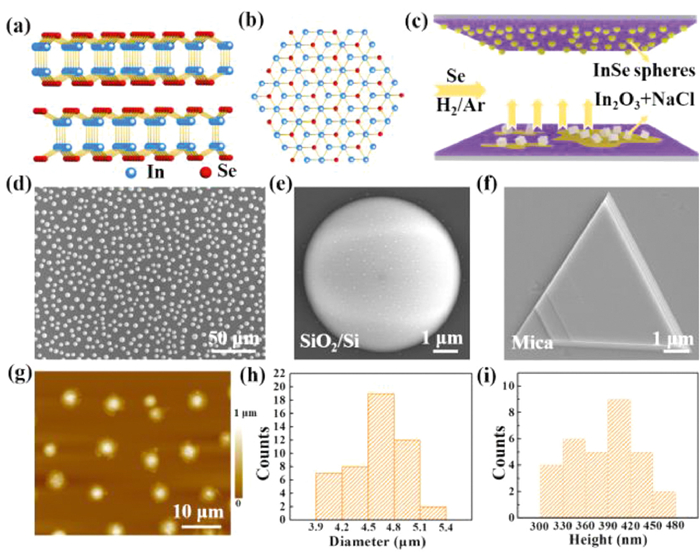
Figs. 1a and b schematically exhibit the side and top views of the atomic structure of the vdW InSe layers. The chemically bonded Se–In–In–Se atoms arrange in a honeycomb lattice within each layer and they are held together by the vdW force. The InSe semisphere array is synthesized by a salt-assisted CVD process [38,39]. The In2O3 precursor along with a certain weight ratio of NaCl was dispersed in NH4OH solution, and then a droplet of the mixed precursor was distributed on a freshly cleaved surface. The growth substrate of SiO2(300 nm)/Si was placed face-down to the precursors with a vertical distance of ~0.5 cm (see Method for the details in Supporting information). The two pieces of substrates create a local environment for the stable precursor sublimation and deposition. The growth was carried out at a temperature of 820 ℃, in which the reaction between NaCl and In2O3 produces the volatile indium oxychlorides and they re-condense onto the SiO2/Si surface in the presence of Se vapor (Fig. 1c). The formation of the InSe spheres was dictated by the VLS conversion mechanism (Fig. S1 in Supporting information), as well as the isotropic and hydrophobic surface properties of the SiO2/Si substrate. As shown in Fig. 1d, densely distributed spheres are observed. Energy dispersive spectroscopy (EDS) image shown in Fig. S2 (Supporting information) and a closer inspection of one sphere reveals the In/Se elements and a perfect semi-spherical topography morphology with the diameter of ~6.4 µm (Fig. 1e). In contrast, when the upper SiO2/Si substrate was replaced by another mica substrate, InSe exhibits the anisotropic growth, presenting triangular and hexagonal shapes (Figs. S3 and S4 in Supporting information). The distinct triangular shape was clearly observed with a lateral dimension of ~6.9 µm (Fig. 1f). In our experiments, the layered InSe crystal shares a similar hexagonal atom structure with the mica substrate (Fig. 1a), so a quasi-epitaxial growth mode could be expected. Moreover, the precursor atoms could migrate easily on the atomically-flat mica substrate, and they tend to move to the most favorable sites under a thermodynamic equilibrium state. Since the InSe inherently owns a hexagonal structure, it is not surprising to obtain the thermodynamic stable shape, i.e., triangular or hexagonal on the mica substrate.
Figure 1
Figure 1.
The growth and morphology characterization of the InSe semispherical array. (a, b) Side and top views of the crystal structure of vdW InSe layers. (c) A schematic diagram of the vapor–liquid–solid growth process of the InSe semispheres. (d) SEM image of the synthesized InSe semispheres on SiO2/Si substrate. (e) An enlarged field-view of one InSe sphere. (f) SEM image of the synthesized multilayer InSe on mica substrate. (g) A representative AFM height image of InSe semispheres. (h, i) Statistics of the diameter and height distribution of InSe semispheres.
The comparative growth study on the two kinds of substrates highlights the role of substrate lattice in guiding the growth behaviors of the deposited materials. On SiO2/Si, due to the amorphous nature of the surface, the materials adopt a liquid-drop like morphology condensed from the precursor vapors. In contrast, the surface lattice guides the crystal growth forming the triangular shape with a straight edge on the mica substrate. In addition, we can prepare atomically-thin InSe nanoflakes on the mica substrate through adjusting the growth parameters (Fig. S5 in Supporting information). The AFM morphology of the InSe spheres was exhibited in Fig. 1g, and the statistical analysis of the diameter and height distribution of the InSe spheres are shown in Figs. 1h and i. The diameters of the InSe spheres are uniform in the range of 3.9–5.4 µm, and the heights span from 300 nm to 480 nm.
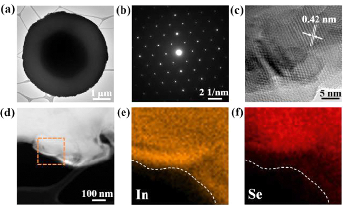
The crystal structure of the InSe semispheres was evaluated by transmission electron microscopy (TEM). The InSe samples for TEM characterizations were prepared by a polycarbonate (PC)-assisted transfer method (see Method). Fig. 2a is a low-magnification TEM image of one InSe semisphere, in which the intact and spherical morphology was maintained after the transfer process. The selected area electron diffraction (SAED) pattern taken from the edge of the sphere indicates the single-crystal nature of the InSe spheres (Fig. 2b), with a hexagonal diffraction pattern corresponding to the atoms arrangement. A high-magnification image of the sample reveals a clear lattice fringe with a lattice spacing of 0.42 nm, which matches well with the (100) crystal plane of InSe (Fig. 2c). Further structural analysis of the samples was tested by X-ray diffraction (XRD) characterization (Fig. S6 in Supporting information). Furthermore, the EDS elemental mappings of part of the InSe semispheres were performed and exhibited in Figs. 2d-f. The uniform distribution of In and Se elements with no detectable amount of impurities in the selected area verifies the successful synthesis of InSe.
Figure 2
Figure 2.
Crystal structure characterizations of InSe semispheres. (a) TEM image of one spherical InSe. (b, c) SAED pattern and a high-magnification image of the spherical InSe. (d) A low-magnification image and (e, f) the corresponding EDS mapping images of part of one InSe sphere.
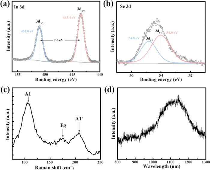
The stoichiometry of InSe semispheres was determined by X-ray photoelectron spectroscopy (XPS). Figs. 3a and b are the XPS spectra for the In 3d and Se 3d core levels and a clear double peak can be fitted for them. The doublet binding energies for In 3d5/2 and In 3d3/2 locate at 443.4 eV and 451.0 eV, respectively, and the spin–orbit interaction leads to a 7.6 eV split.
Figure 3
Figure 3.
Spectroscopy measurements of the synthesized InSe semispheres. (a, b) The core level XPS spectra for (a) In 3d and (b) Se 3d. (c) Raman spectrum of InSe semispheres recorded using a 514 nm laser at room temperature. (d) Photoluminescence of the InSe sample.
The binding energies of Se 3d5/2 and 3d3/2 are 54.0 eV and 54.8 eV, respectively, in agreement with those of the bulk InSe materials. Raman spectroscopy as a non-destructive technique was used to probe the optical properties of the synthesized InSe spheres. Three prominent peaks appearing at 108 cm−1 (A1 mode), 175 cm−1 (Eg mode), and 208 cm−1 (A1′ mode) are consistent with the Raman feature of the InSe materials (Fig. 3c). In addition, the PL spectrum was also acquired with an excitation laser wavelength of 514 nm. The spectrum exhibits an obvious peak at ~1144 nm (Fig. 3d), corresponding to an optical bandgap of ~1.1 eV.
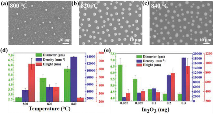
The formation of the InSe semispheres could be well explained by the VLS growth mechanism [40]. At the growth temperature of 820 ℃, the reaction between the precursor In2O3 and the NaCl salt results in the formation of volatile In2O3-xClx vapor, which recondense onto the upper substrate to form the liquid droplet. As the Se vapor is brought by the H2/Ar carrier gas, the dissolution of Se and the reaction between Se and In2O3-xClx droplets give rise to the formation of InSe semispheres. As such, controlling the reaction parameters including growth temperature and precursor amounts is of vital importance for adjusting the spheres density and morphology. For example, Figs. 4a-c exhibit the SEM images of the growth results performed at 800 ℃, 820 ℃, and 840 ℃. As the growth temperature increases, more precursor vapor generation and condension onto the growth substrate occurs, resulting in an increased spheres density and larger sphere diameters (Fig. 4d). Correspondingly, the average height of the InSe spheres decrease. The influence of the In2O3 precursor amount on the spheres density and size was also investigated. For specific statistics, see Table S1 (Supporting information). Fig. S7 (Supporting information) exhibits the SEM images of the growth results performed at 0.065 mg, 0.085 mg, 0.1 mg, 0.2 mg, and 0.3 mg. The InSe spheres density and height increase along with the increased amount of the In2O3 precursor and the diameter decreases simultaneously (Fig. 4e and Table S2 in Supporting information). These parameters adjustment provides tunable ways for controlling the InSe spheres with varied density, morphology, and size.
Figure 4
Figure 4.
The influence of the growth parameters on the density and size of the InSe semispheres. (a-c) SEM images of the InSe semispheres grown at the temperatures of 800 ℃, 820 ℃, and 840 ℃. (d) A statistical analysis of the InSe spheres density, diameter, and height as a function of growth temperature. (e) A statistical analysis of the InSe spheres density, diameter, and height as a function of In2O3 precursor amount.
The InSe semisphere array was used as HER catalyst in following electrochemical tests. In acidic medium as in our experiments, two continuous steps have been proposed for electrocatalytic HER. The Volmer (H3O+ + e−→ Hads + H2O) reaction is the first step. When HER starts, hydronium ions (H3O+) are adsorbed on the surface of the sample, and electrons on the cathode surface are coupled with (H3O+) to form adsorbed hydrogen (Hads). After that, the Heyrovsky (Hads + H3O+ + e− → H2 + H2O) reaction or the Tafel (Hads + Hads → H2) reaction occurs to generate hydrogen molecules. To keep the array intact, the samples are directly transferred from the growth substrate onto the Au film deposited on Si substrate (see Method). The bare Au film electrode was also tested as a reference. Moreover, the liquid-phase exfoliated InSe flakes from the vdW InSe bulk powder were tested in order to compare the performance between the gas-phase and liquid-phase derived samples, and also the comparison of behaviours between different morphologies. It is noted that we have also attempted to transfer the InSe flakes grown on mica to Au film electrode as a control sample, but the interaction between the InSe flakes and the mica substrate was too strong to be exfoliated and all the transfer attempts failed. The spherical morphology of InSe was believed to provide more edge sites for the intermediate adsorption during the catalytic reaction as compared with the flakes with the same surface area [41,42].
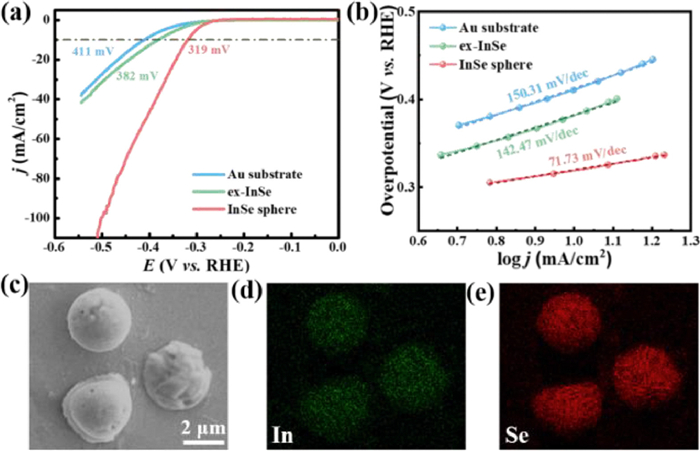
The SEM image of InSe flakes are shown in Fig. S8 (Supporting information). The Raman spectroscopy of InSe flakes is shown in Fig. S9 (Supporting information). The polarization curves and Tafel plots from the above three samples (Au substrate, InSe flake, and InSe sphere) are shown in Figs. 5a and b. The overpotential of Au electrode at 10 mA/cm2 is 411 mV and that of InSe flake is 382 mV, indicating the presence of electrocatalytic active site in the InSe flake samples. The InSe semisphere exhibits the lowest overpotential of 319 mV at 10 mA/cm2 and an obviously higher current density, which demonstrates the superior HER performance than the Au substrate and InSe flake samples. The Tafel slopes of InSe semisphere, InSe flake, and Au substrate are 71.73 mV/dec, 142.27 mV/dec, and 150.31 mV/dec, respectively, in line with the polarization curves. The improved performance of the InSe semispheres may originate from the fully exposed InSe spherical surface with abundant adsorbing sites (Fig. S10 in Supporting information), as well as the high crystal quality for the electron transport in comparison with the InSe flake samples. The transferred InSe semispheres after the HER tests for 20 times were also characterized. The compact spherical morphology and the uniform distribution of the In and Se elements within the spherical areas indicate the stability of the gas-phase derived InSe spheres (Figs. 5c-e). The comparison of the polarization curves of the samples before and after 50 testing cycles further suggests the good stability of the structure (Fig. S11 in Supporting information). The improved stability of the InSe spheres might also benefit from the higher crystal quality of the gas-phase synthesized samples, which could effectively block the penetration and reaction with the electrolytes.
Figure 5
Figure 5.
HER performance of the InSe semispherical array. (a) Polarization curves of as-synthesized InSe semisphere, InSe flake, and the reference Au substrate in 0.5 mol/L H2SO4. (b) Tafel plots of the curves in (a). (c) SEM image of the InSe spheres after HER tests for 20 times. (d, e) In and Se elemental mappings from the same area in (c).
In summary, the salt-assisted vapor–liquid–solid growth of a new morphological main group metal chalcogenide (MMCs), InSe semispherical array with uniform size and distribution, is demonstrated in this work. The growth mechanism was studied by varying the growth parameters, along with the density and size of the semispheres being controllably adjusted. The InSe semispheres with exposed edges on surface and high crystal quality are suitable for application as an electrocatalyst in hydrogen evolution, which exhibited superior performance than the liquid-exfoliated 2D InSe flakes. The growth method reported here could be expanded to the synthesis of other MMCs and the derived samples could also be applied to other high-performance electrocatalytic reactions.
Declaration of competing interest
The authors declare that they have no known competing financial interests or personal relationships that could have appeared to influence the work reported in this paper.
Acknowledgments
We thank the financial support from the National key R & D Program of China (No. 2021YFA1202802), Beijing Municipal Natural Science Foundation (No. 1212016), National Natural Science Foundation of China (Nos. 22104109 and 12102098), the CAS Pioneer Hundred Talents Program, and China Postdoctoral Science Foundation (Nos. 2020M680479, 2021M690801).
Supplementary materials
Supplementary material associated with this article can be found, in the online version, at doi:10.1016/j.cclet.2022.107826.
[1]
M. Xu, T. Liang, M. Shi, et al., Chem. Rev. 113 (2013) 3766–3798. doi: 10.1021/cr300263a
[2]
T. Lu, T. Li, D. Shi, et al., SmartMat 2 (2021) 591–602. doi: 10.1002/smm2.1063
Figure 1
The growth and morphology characterization of the InSe semispherical array. (a, b) Side and top views of the crystal structure of vdW InSe layers. (c) A schematic diagram of the vapor–liquid–solid growth process of the InSe semispheres. (d) SEM image of the synthesized InSe semispheres on SiO2/Si substrate. (e) An enlarged field-view of one InSe sphere. (f) SEM image of the synthesized multilayer InSe on mica substrate. (g) A representative AFM height image of InSe semispheres. (h, i) Statistics of the diameter and height distribution of InSe semispheres.
Figure 2
Crystal structure characterizations of InSe semispheres. (a) TEM image of one spherical InSe. (b, c) SAED pattern and a high-magnification image of the spherical InSe. (d) A low-magnification image and (e, f) the corresponding EDS mapping images of part of one InSe sphere.
Figure 3
Spectroscopy measurements of the synthesized InSe semispheres. (a, b) The core level XPS spectra for (a) In 3d and (b) Se 3d. (c) Raman spectrum of InSe semispheres recorded using a 514 nm laser at room temperature. (d) Photoluminescence of the InSe sample.
Figure 4
The influence of the growth parameters on the density and size of the InSe semispheres. (a-c) SEM images of the InSe semispheres grown at the temperatures of 800 ℃, 820 ℃, and 840 ℃. (d) A statistical analysis of the InSe spheres density, diameter, and height as a function of growth temperature. (e) A statistical analysis of the InSe spheres density, diameter, and height as a function of In2O3 precursor amount.
Figure 5
HER performance of the InSe semispherical array. (a) Polarization curves of as-synthesized InSe semisphere, InSe flake, and the reference Au substrate in 0.5 mol/L H2SO4. (b) Tafel plots of the curves in (a). (c) SEM image of the InSe spheres after HER tests for 20 times. (d, e) In and Se elemental mappings from the same area in (c).

 DownLoad:

 下载:
下载:


