Citation:
Ziyang Yin, Lingbin Xie, Weinan Yin, Ting Zhi, Kang Chen, Junan Pan, Yingbo Zhang, Jingwen Li, Longlu Wang. Advanced development of grain boundaries in TMDs from fundamentals to hydrogen evolution application[J]. Chinese Chemical Letters,
2024, 35(5): 108628.
doi:
10.1016/j.cclet.2023.108628
Advanced development of grain boundaries in TMDs from fundamentals to hydrogen evolution application
English
Advanced development of grain boundaries in TMDs from fundamentals to hydrogen evolution application
College of Electronic and Optical Engineering & College of Flexible Electronics (Future Technology), Nanjing University of Posts & Telecommunications (NJUPT), Nanjing 210023, China
b.
Institute of Advanced Materials (IAM) & Institute of Flexible Electronics (Future Technology), Nanjing University of Posts & Telecommunications (NJUPT), Nanjing 210023, China
* Corresponding authors. E-mail addresses: zhit@njupt.edu.cn (T. Zhi)
Received Date:
14 April 2023 Accepted Date:
29 May 2023 Revised Date:
06 May 2023 Available Online:
15 May 2024
Abstract:
Grain boundary (GB), as a kind of lattice defect, widely exists in two-dimensional transition metal dichalcogenides (2D TMDs), which has complex and diverse influences on the physical/chemical properties of 2D TMDs. GBs are universally considered to be a double-edged sword, although some electrical and mechanical properties of 2D TMDs would be adversely affected leading to the reduced overall quality, certain structure-oriented applications could be realized based on its unique properties. In this review, we first detailed the atomic structure characteristics of GBs and the corresponding techniques, then we systematically summarized the methods of introducing GBs into 2D TMDs. Next, we expounded unique electrical, mechanical, and chemical properties of the GBs in 2D TMDs and clarified its internal relationship with the atomic structure. Moreover, the application of GB structure in hydrogen evolution reaction (HER) is also discussed. In the end, we make a conclusion and put forward outlooks, hoping to further promote the basic research of GB and boost the wide application of 2D TMDs.
In recent years, 2D TMDs represented by MoS2 have attracted great attention due to their unique electronic [1], optical [2-4], thermal [5], catalytic [6], mechanical [7] and other characteristics [8], and have been widely applied in field effect transistors [9,10], sensors [11-14], photodetectors [15], flexible electronic devices [16] and other applications [17-21]. In addition, it is well known that HER is a key process of hydrogen production by electrocatalysis and photocatalysis, in which catalyst plays a decisive role to improve the reaction rate [22-24]. Although Pt and Pt-based noble metal catalysts can significantly reduce the overpotential to improve the catalytic activity, their wide applications as catalysts are limited by the scarcity and high cost [25-27]. In view of the characteristics low cost, high stability and good soil abundance, TMDs are considered to be the most promising non-noble metal hydrogen evolution catalysts to replace Pt and Pt-based catalysts [28-32]. In order to fully realize the full application potential of TMDs, it is of great necessity to develop large-scale and reliable preparation methods. Through the current preparation methods, defect structures will inevitably be introduced in the process of growth and synthesis of 2D TMDs, which has a nonnegligible impact on their properties that cannot be ignored [33].
Grain boundaries (GBs) can usually be described as line defects consisting of a series of dislocations arranged to connect different grain regions [34]. Based on all kinds of advanced characterization technologies such as high-resolution transmission electron microscopy (HRTEM), atomic force microscopy (AFM) and scanning tunneling microscopy (STM), a growing number of studies have explicitly revealed the atomic structure characteristics of GBs. Various fabrication strategies (top-down, bottom-up) have been developed to purposefully synthesize materials rich in GBs. Taking 2D materials with this fixed structure characteristics as a model, increasing numbers of physical and chemical properties related to GBs are disclosed. For example, GBs will hinder the conductivity and carrier mobility of 2D TMDs [35,36], and the existence of GBs will introduce electric fields and strain fields in the vicinity [37], leading to the variety of photoluminescence (PL) intensity. These unique properties and features also suggest that GBs have great application potential in functional devices [38,39]. In the field of catalysis, GB could directly act as active sites due to its unique atomic structure [40,41]. In addition, the atomic structure would change the properties of the material, affecting the catalytic activity [42]. At the moment, it has been proved that GBs do have significant applications in the field of hydrogen production both from the perspective of theoretical calculation and experiment.
In this paper, we first discuss the atomic structure of GBs, then summarize some methods for preparing GB-rich TMDs and characterizing GBs rapidly and effectively. Finally, the electronic, optical, thermal and mechanical properties of GBs and some experimental and theoretical research results in the application of HER are discussed. We sincerely hope that this review can help researchers establish a deeper understanding of the GBs in TMDs and further promote the development of this promising material.
2.
Atomic structure and characterization
In 2D TMDs, the splicing of crystals with various orientations created by various nuclei and seeds results in the formation of GBs, which can be described as arrays of dislocations. And technologies of obtaining the global distribution and atomic resolution imaging of GBs in 2D materials has also been developed for comprehensive understanding of its rich morphology.
2.1
Atomic structure
The TMDs composed of Mo, W metal atoms and S, Se chalcogenides are layered structure in bulk, having covalently-bonded X–M–X (M = Mo, W; X = S, Se) in each atomic plane with adjacent layers coupled by weak van der Waals forces [43-45]. According to their dimensions, the fundamental defect types in 2D TMDs can be separated into point defects and one-dimensional defects [46-48]. One-dimensional defects with different crystal directions on both sides are widely defined as GBs, which can usually be described as an array composed of a series of dislocations [49]. In addition to the 5|7 dislocation core, different dislocation cores such as 4|6, 6|8, and 4|8 were observed at GB in 2D TMDs. Understanding the atomic structure of GBs and the dislocations that make up GBs is crucial since they are indispensable in 2D TMDs and significantly affect characteristics. Dislocations may undergo mutual transformation and migration in some particular situations, which has a profound effect on the structure of GBs.
2.1.1
Atomic structure of dislocation core
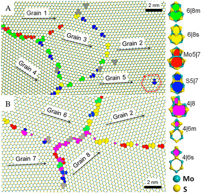
GBs are usually formed during the growth or kinetic processing of TMDs [50], and best characterized as a collection of dislocation cores when the misorientation angle is modest [51]. As shown in Figs. 1A and B, unlike the GBs in graphene, which are usually composed of 5|7 dislocations, GBs in 2D TMD materials can be composed of local 4|4, 5|7, 6|8 structure units and other dislocations [52]. In GBs with intermediate misorientation angles, 5|7 and 6|8 dislocations coexist, and the misorientation angle affects both the type and density of the dislocation. For instance, in Fig. 1A, the high-angle tilt GB separating grains 1 and 4 is made up predominantly of isolated 5|7 dislocations, whereas the low-angle tilt GB separating grains 2 and 5 is made up primarily of dense 5|7 and 6|8 dislocations. In addition, due to the heterogeneity of the structure, 2D TMDs easily to show element polarity at the growth front when they are prepared by chemical vapor deposition (CVD). In general, the S-rich 5|7 type of dislocation is labeled as S5|7, whose structural feature is that there are two S-S homoelemental bonds at the center of the dislocation core. Similarly, Mo-rich 5|7 (Mo5|7) has two Mo-Mo homoelemental bonds to connect five- and seven-membered rings. Given the fact that S-S and Mo-Mo homoelemental bonds are less advantageous energetically than S-Mo heteroelemental bond, the 6|8 dislocations can be formed by inserting Mo or S into the homoelemental bonds of 5|7 dislocations. In contrast, the 4|6 dislocations can be generated from 5|7 dislocations by deleting Mo or S that originally form the homo-elemental bonds.
Figure 1
Figure 1.
Grains and GB structures in 2D polycrystalline MoS2. (A) Typical loop and (B) Y-shaped GBs captured from the polycrystal. The black arrows indicate the zigzag direction of bulk of grain. Boundary misorientation angles are explained by the angles between the arrow vectors in the neighboring grains. GBs are composed of diverse dislocation cores, depending on boundary misorientation angles. The right side shows typical dislocation cores captured from GBs in polycrystal, and they are individually named according to the feature of ring pairs for clarification. Reprinted with permission [52]. Copyright 2018, American Chemical Society.
It is generally known that the atoms in GBs are energetically unfavorable compared to those in pristine crystal. According to previous experiments and studies, dislocations will migrate under the influence of external conditions such as temperature, electronic doping or mechanical stretching. The migration of dislocations not only affects the electronic, mechanical and magnetic properties of 2D TMD materials, but is also crucial in changing the durability and performance of large-scale nanodevices and memristors made of polycrystalline 2D TMDs.
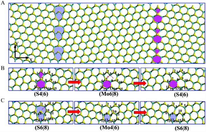
Liu et al. discussed the effect of temperature on the mobility of GBs in MoS2 thin films [53]. Fig. 2A shows two different types of dislocations, S4|6 and S6|8. Since the energy of homo-bonds is lower than that of S-Mo hetero-bonds, 5|7 dislocations can react with interstitial S or S vacancy to form S4|6 and S6|8. The experimental results show that the response of GB motion to temperature becomes stronger and the migration barriers of dislocations decrease when the temperature increases. The films containing S4|6 and S6|8 GBs are more sensitive to temperature changes, and the dislocations that occupy the main part constantly migrate and transform. It is seen that the S4|6 GB fluctuates between S4|6 and Mo6|8 configurations, whereas the S6|8 GB fluctuates between S6|8 and Mo4|6 configurations, neither variation has a favored migration direction. Although there is no clear directivity, they show a high mobility (Figs. 2B and C). In contrast, Mo5|7 GBs will not migrate even under the influence of a strong thermal field.
Figure 2
Figure 2.
(A) MoS2 film with S4|6 and S6|8 GBs. (B) Migration process of S4|6 GB. (C) Migration process of S6|8 GB. The different GBs are filled with different colors. Reprinted with permission [53]. Copyright 2020, The Royal Society of Chemistry.
Electronic doping can reduce the potential barrier of dislocation migration [54]. The first-principal calculation shows that electron doping can reduce the migration barrier by approximately 50%, which is mainly controlled by the change of the occupancy of the defect energy levels around the Fermi level during dislocation migration.
Moreover, two different types of damage, brittle and ductile, may occur after the in-plane tension is applied to the GBs in the single-layer MoS2 film [55]. The brittleness failure is characterized by the gradual dissociation of bonds at GBs, while the ductile failure is characterized by the migration of dislocations. When uniaxial strain is applied, a series of structural changes will take place. The Mo-S bonds are further dissociated once the S-S bonds that are shared by 5|7 dislocations are first broken apart. Then unsaturated S atoms will react with the surrounding Mo atoms to produce 4|8|6 clusters when the tension reaches the critical value, and in order to eliminate redundant strain, S4|6 and S6|8 are spontaneously generated.
2.2
Characterization
GBs are ubiquitous in large-area as-grown TMD materials, and have important influences on the properties of 2D TMDs, so developing fast and sensitive characterization methods to visualize GBs is of great importance. Up to now, various characterization methods, including optical microscopy [56], PL mapping [57], AFM [58], scanning electron microscopy (SEM) [59], aberration-corrected annular dark-field scanning transmission electron microscopy (ADF-STEM), STM [60], and HRTEM [61], have been applied for atomic scale characterization of GB structure in TMDs [62].
2.2.1
Optical microscopy
Optical microscopy can quickly provide the position, shape and thickness of materials, so the visibility of 2D TMDs under ordinary optical microscopy greatly promotes the in-depth study of their characteristics and applications. At present, optical imaging technologies based on the unique nonlinear optical properties of 2D TMDs have also been developed, which can quickly and sensitively characterize the defect structure.
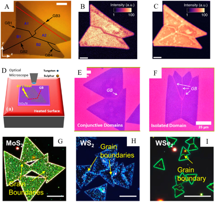
To date, optical nonlinear second harmonic techniques (SHG) and third harmonic techniques (THG) have been developed to observe GBs. Compared with the centrosymmetric materials which are not affected by the second-order nonlinear process, the broken inversion symmetry of the crystal structure in odd-layer MoS2 makes it exhibit strong second harmonic generation. The destructive interference of nonlinear waves between adjacent atomic films revealed a small number of GBs connecting different crystals. Because this nonlinear oscillation is unique to layered TMDs such as MoS2, this optical imaging technology has been used to rapidly map them over a large range. However, this technology is only applicable to the detection of GBs in odd-layer MoS2 sheets. When the MoS2 sheet is an even layer, its crystal structure has central symmetry and cannot generate SHG signals. On the premise that monolayer MoS2 can generate third harmonic waves under the excitation of infrared ray, Lasse karvonen et al. proved that THG can be effectively used to detect GBs in MoS2 grown by CVD, and this technology has good sensitivity and a fast response time [63]. The most important advantage of this technology compared with SHG is that both odd-layer and even-layer MoS2 films can be quickly and accurately identified. Second, the SHG field between adjacent grains may have destructive interference, and the weakening of this signal may lead to the loss of some GBs in the final recognition image. Fig. 3A shows the optical wide field image of the sample and highlights the observed grains and GBs. Take Fig. 3C as an example, in the THG image, all four GBs are clearly visible. However, in the SHG image, GB1 and GB4 are clearly visible, GB2 has low brightness, and GB3 is almost invisible. The origin of the SHG signal is in the asymmetric crystal structure of MoS2 and the destructive interference of the SHG fields from the neighboring grains leading to GB1 appearing dark in the image (Fig. 3B). In addition, because THG signal is sensitive to the solvent used in CVD process, the combination of solvent and laser scanning can greatly improve the contrast of THG signals between GBs, making them easier to detect. We can quickly and conveniently identify GBs in large-sized MoS2 samples produced in industry without causing any damage to the sample itself, but it will fail when the torsion angle approaches zero.
Figure 3
Figure 3.
(A) Optical image with marked grains (A1, A2, B1 and B2) and GBs (GB1, GB2, GB3 and GB4). (B) Experimental SHG image without analyser. (C) Experimental THG image without analyser. Reprinted with permission [63]. Copyright 2017, Springer. (D) Schematic illustration of the thermal treatment that enabled direct imaging of WS2 GBs using an optical microscope. (E, F) Optical images of WS2 GBs in other monolayer configurations of the as-formed WS2 crystal. Reprinted with permission [64]. Copyright 2015, American Chemical Society. (G–I) Dark-field optical images of MoS2, WS2, and WSe2. Scale bar is 20 µm. Reprinted with permission [65]. Copyright 2015, American Chemical Society.
Additionally, in order to characterize the GBs in TMD samples more clearly with optical microscopy, some pretreatment methods can be taken. Fig. 3D shows the schematic diagram of heat treatment, the controlled air heating of the TMD film samples grown by CVD method will cause local structural changes of the GBs in the samples, resulting in strong contrast lines in the GB area during observation [64]. As shown in Figs. 3E and F, after heat treatment, strong contrast lines are displayed at the position of GBs in WS2 domains. However, it should be pointed out that the heating time and temperature are of great importance in the observation. The comparison of experimental results shows that the GBs in the sample are most clearly identified after heating at 380 ℃ for 20 min. If the heating temperature is further increased or the heating time is prolonged, the structure of the GBs in the sample will be damaged. At the same time, the environment of growing and processing single-layer WS2 films will also have some influence on the observation.
By anchoring silver nanoparticles at the defect sites of MoS2 samples, visualization of the distribution of GBs in single-layer TMD films can be achieved by using dark field optical microscopy [65]. As shown in Figs. 3G–I, due to the enhanced light scattering at defects under dark field conditions, the distribution of GBs in single-layer TMD samples has been clearly visualized.
2.2.2
Scanning probe microscopy and electron microscopy
Among various material characterization technologies, electron microscopy, including transmission electron microscopy (TEM), scanning transmission electron microscopy (STEM), and ADF-STEM has been proven to be a universal and valuable method that can detect the distribution of various microstructures and defects in 2D TMDs at the atomic scale. Compared with the commonly used TEM, STEM uses a highly focused electron beam for imaging and analysis, while annular dark-field imaging, also known as Z-contrast imaging, uses atomic number contrast to display atomic scale structure information. Scanning probe microscopy is the general name of various microscopies developed on the basis of STM. STM and AFM are two kinds of scanning probe microscopy commonly used. STM detects the surface structure of the sample by measuring the tunnel current between the probe and the tested sample. AFM detects the surface of the sample by detecting the microcantilever deformation caused by the interaction between the tip and the sample through the photoelectric displacement sensor. The resolution of STM parallel to and perpendicular to the surface is 0.1 nm and 0.01 nm respectively, while the resolution of AFM is approximately tens of nm. At present, both of them have been extensively used in characterizing defects in 2D materials and reveal the surface morphology at the atomic level.
Ly et al. found that when TMD films grown on sapphire substrates are exposed to ultraviolet radiation under humid conditions, oxygen and hydrogen radicals will be generated (Fig. 4A). The original width of the GBs is very narrow, but these free radicals subsequently oxidized defective GBs, expanding the width, so that AFM and SEM can observe this morphological modification [66]. As shown in Figs. 4B and D, the GBs cannot be directly observed in the image of pristine samples. After six minutes of ultraviolet irradiation, the GBs in the sample are oxidized, and this morphological change can be clearly observed in both the AFM and SEM images (Figs. 4C and E). It should be noted that the ultraviolet irradiation method easily damages the structure of the GBs in the process of oxidation if the exposure time is too long. However, considering its short recognition time, it can be generally applied in the rapid identification of the GBs.
Figure 4
Figure 4.
(A) Schematic diagram for UV treatment monolayer WSe2. (B, C) AFM and SEM image of pristine WSe2. (D, E) AFM and SEM image of oxidized WSe2 after 6 min UV treatment. Reprinted with permission [66]. Copyright 2014, American Chemical Society. (F) In the large-scale STM image, the 6° GB is meandering and aperiodic (100 × 100 nm2; scale bar, 10 nm; Vtip = −1.2 V), where the insets (i) and (ii) reveal the different lattice orientations for the corresponding domains (each inset: 3 × 3 nm2; scale bar, 1 nm; Vtip = 0.6 V). (G) Another aperiodic GB with a misorientation angle of 3° (60 × 60 nm2; scale bar, 10 nm; Vtip = −1.0 V). Reprinted with permission [67]. Copyright 2016, American Chemical Society. (H) High-resolution ADF-STEM image of a mirror twin boundary. The boundary is visible just below the annotated line. The annotation indicates the nanoscale faceting of the boundary at ±20° off the zigzag direction. (I) Zoomed-in image of the GB shows a periodic line of 8-4-4 ring defects. (J) An atomistic model of the experimental structure shown in (I). Reprinted with permission [68]. Copyright 2013, Springer.
As a means of characterization with atomic level accuracy, STM has been widely used in the research of 2D materials. Huang et al. successfully characterized GBs in single-layer WSe2 with STM [67]. Figs. 4F and G characterized GBs with different misorientation angles in the sample, but only low-angle GBs with misorientation angles smaller than 10° were observed in the single-layer WSe2 sample. This may be caused by the fact that the temperature can reach as high as 900 ℃ in the process of CVD growth, while the structure of GBs with large misorientation angles is relatively unstable under a high-temperature environment. In addition, it can be seen from Fig. 4G that the GBs are composed of a series of bright protrusions. These bright protrusions are dislocation cores in essence, and the spacing between dislocation cores will increase with decreasing misorientation angle.
Aberration-corrected ADF-STEM was also used to obtain an atomic resolution image of MoS2, where detailed grain and GB structures were revealed [68]. Fig. 4H shows a mirror twin boundary. The GB follows the zigzag direction, and the nanoscale faceting of the boundary at ±20° off the zigzag direction. It can be clearly seen in Figs. 4I and J that the GB is mainly composed of eight- and four-membered rings. In previous reports, GBs can also be composed of a line of 5–7 rings. This further proves that both even element rings and odd element rings can form GBs in TMDs.
It is worth mentioning that in order to more clearly visualize GBs in TMDs, some methods can be taken to assist the observation. Besides ultraviolet irradiation and high temperature heating, hot water vapor etching can likewise provide assistance to visualize GBs at large scales [69]. After exposure to mild water vapor, the GBs in TMDs were oxidized, which enhanced their optical contrast. This technology takes advantage of the reactivity difference between GBs and grain domains in TMDs, and is almost non-invasive. Similar to the previously reported use of hydrofluoric acid (VHF) etching to observe the GBs in graphene placed on the SiO2 substrate, after the MoS2 on the SiO2 surface is exposed to VHF, the VHF molecules will diffuse through the lattice structure of GBs, and lead to the etching of SiO2. Due to the difference between the etching speed of SiO2 at GBs and in non-GB areas, the resulting patterns can be clearly observed by electron microscopy or optical microscopy. However, as an invasive method, it is easy to damage the GBs in MoS2.
2.2.3
Photoluminescence mapping
As a non-destructive and sensitive analytical method, PL can reveal details about the structure, composition and atomic arrangement of materials. Due to the obvious heterogeneity of the PL characteristics of defects in 2D TMDs, PL mapping can visualize defects such as GBs in materials. However, it needs to collect a wide spectrum within a specific wavelength range at each measuring point, and is not suitable for characterizing large area samples.
The work of Liu et al. shows that PL mapping can also be used as a non-contact method to quickly identify GBs in MoS2 [70]. Fig. 5A shows a representative polycrystalline MoS2 sample. After PL intensity mapping, it is found that the PL intensity at GBs is high, which can be highlighted (Fig. 5B). In order to explore its principle, five positions were selected on the straight line (Fig. 5C) to collect PL spectra separately. Two points are located at the GB and three points are located in the pristine MoS2 region. It can be clearly seen from Figs. 5D and E that the PL strength of 2 and 4 is obviously greater than that of 1, 3 and 5, proving that the PL strength at the GB has been greatly enhanced. Fig. 5F shows the line profile of the peak position, where the peak displacement of PL at the GB is approximately 5 meV, while at the edge is about 15 emV. This small blue shift indicates that the behavior of defects at the GB is very similar, and the change of PL characteristics in the single-layer MoS2 is likely caused by the strain at GBs. This is also proven by the low-temperature PL spectra of the GB region and non-GB region.
Figure 5
Figure 5.
PL characterization of polycrystalline MoS2 star with twin GBs. (A) Optical image of a MoS2 star sitting on SiO2. (B) PL intensity mapping. The edges and twin GBs have a higher intensity (light yellow), while rest are depicted in orange. (C) PL peak position mapping. PL spectra are collected at the location marked five dots with different colours. Scale bar: 3 µm. (D) PL spectra collected from points indicated in (C). Each spectrum corresponds to the location in (C) with the same color. (E, F) PL intensity and peak position line profiles as indicated by the white dash lines crossing two GBs and two edges. Reprinted with permission [70]. Copyright 2014, Springer.
It can be seen that an increasing number of methods have been used to characterize the atomic structure and distribution of GBs in 2D TMDs, and their types and characteristics have been fully revealed.
3.
Fabrication method
The main methods used to prepare 2D TMD nanosheets include mechanical exfoliation [71,72], liquid phase exfoliation [73,74], intercalation exfoliation, CVD [75-77], hydrothermal method [78-80], electrochemical exfoliation [81-83], pulsed laser deposition (PLD) [84,85], molecular beam epitaxy [86-88] and colloidal synthesis, etc. Due to the weak van der Waals force between layers of layered compounds, the mechanical exfoliation method realizes the separation of nano layers by applying mechanical forces such as friction and tension to layered crystals. Although the sample produced by this approach is comparatively pure, due to its poor yield, it is not suitable for large scale preparation. The electrochemical exfoliation method often affects the electrical properties of samples in the preparation process. Ultrasonic waves are typically needed to treat the samples in the conventional liquid phase exfoliation, and the nano sheets prepared are small in size. CVD is anticipated to achieve large-scale production of TMD nanosheets through continual optimization and innovation of preparation techniques [89]. The grain size of TMD films grown by these technologies usually ranges from several hundred nanometers to several millimeters, resulting in low GB density. To date, the main methods used to prepare atomic thin GB-rich TMD films are CVD, hydrothermal method, PLD, direct laser writing, electron/ion irradiation and so on.
3.1
Bottom-up strategies
By and large, the strategies of introducing GBs into single-layer TMD materials through defect engineering have been widely studied. Its fabrication strategies can be roughly divided into two types: bottom-up and top-down. Bottom-up strategies can directly form specific types of defects in the process of material preparation, which is also commonly referred to as one-step or in-situ synthesis method [90]. For the introduction of GB, the first method is to use CVD. By controlling the vapor phase in the chemical reaction, solid material films are epitaxially deposited on the substrate surface. MoS2 thin films prepared by CVD method are usually polycrystalline, with grain sizes ranging from 1 microns to 10 microns. The second method is hydrothermal method, which usually uses molybdate and sulfide to react in autoclave, and a series of chemical and physical reactions occur at relatively high temperature and pressure. The third method is PLD, in which the physical reaction has a significant impact on the non-equilibrium process including nucleation, so it is considered as an effective method to grow TMD materials into van der Waals heterostructures.
In current industrial scale preparation methods, CVD is an effective method to manufacture large area and high-quality materials [91]. Compared with other exfoliation methods, although the quality of samples produced by CVD is slightly lower, it has significant advantages in manufacturing speed and preparation scale, and is more suitable for being developed as a method of large-scale production in industry [92]. The single-layer MoS2 samples prepared by CVD have multiple nucleation sites, which will generate GB regions between grains.
On the basis of CVD, He et al. successfully prepared atomic thin TMD films with high GB density by using the method of Au-quantum-dots assisted vapor-phase growth [93]. Fig. 6A shows the growth process of the wafer-scale film. First, by heating the Au film on SiO2/Si substrate at high temperature, an Au quantum dots layer with ultra-high density was prepared. During the process, the initial deposition time of the Au film is vital to the final size and density of the Au quantum dots. With the increase of deposition time, the size of Au quantum dots will increase and the density will decrease. MoS2 thin films were then grown on the basis of Au quantum dots using vapor growth technology, and finally, the Au quantum dots were removed from the MoS2 thin films using etchants at ambient temperature, thus successfully obtaining MoS2 thin films with ultra-high density of GBs. Raman spectra of the obtained MoS2 films revealed that the intensity of in-plane mode and out-of-plane mode is relatively small, indicating that the prepared films are polycrystalline and have a high GB density. During the whole growth process, Au quantum dots controlled the formation of grains in TMD films by limiting the size of TMD domains and promoting the nucleation of TMD films.
Figure 6
Figure 6.
(A) Schematic of the wafer-scale growth of TMD nanograin films. Ultra-high-density Au quantum dots (QDs) were used to grow the MoS2 (as well as WS2 atom-thin films: see Supporting information). Reprinted with permission [93]. Copyright 2020, Springer. (B) Schematic diagram of synthetic high-density dislocation intrinsic flexible MoS2 nanosheets. Reprinted with permission [94]. Copyright 2022, Springer. (C) Schematic of a conventional PLD setup. Reprinted with permission [96]. Copyright 2021, Elsevier. (D) High-resolution ADF STEM image of a 180° twin GB showing a periodic line of defects with 4|8 motif rings. The overlaid triangles denote the twin grains rotated by 180° with respect to each other. (E) Simulated STEM image of a GB relaxed structure reproducing the 4|8 structure. The yellow scale bar has a length of 5 Å. Reprinted with permission [97]. Copyright 2021, American Chemical Society.
Hydrothermal synthesis can also introduce a significant number of dislocations and GBs in the preparation of MoS2 thin films, and the method is easy to implement. Wang et al. successfully prepared MoS2 nanosheets containing a large number of in-plane and out-of-plane dislocation structures using the strategy of low-temperature hydrothermal synthesis [94]. Fig. 6B shows the preparation process of MoS2 nanosheets. Ammonium molybdate tetrahydrate and thiourea were put into the reactor as precursors, and high-density dislocations were introduced after ten days of low-temperature hydrothermal treatment at 120 ℃. Under the condition of low temperature, the two clusters of vulcanized products are spliced together in disorder, finally a MoS2 nanosheet with low crystallinity is gradually formed and a large number of dislocation defects are introduced. The distribution of in-plane dislocations is obtained after the fast Fourier transform, and the GB structure dominated by 5|7 dislocations is observed. Due to its abundance of in-plane and out-of-plane dislocation defects, the MoS2 nanosheet also demonstrates excellent catalytic activity and long-term stability in HER. This further reveals that GBs and dislocations will have an impact on the catalytic performance of TMDs in HER, a topic that will be covered in more detail later.
Pulsed laser deposition, also known as pulsed laser ablation, is an effective method to grow 2D TMDs into van der Waals heterostructures [95]. The film produced by this method has high uniformity, can realize small scale film deposition, and has a rapid reaction [96]. Therefore, PLD has great development potential. Fig. 6C shows the schematic diagram of PLD growth. The intended target is first exposed to the ultraviolet laser beam, and then the produced plume rises. Finally, the film is deposited on the substrate that maintains the desired temperature. Although this production method has advanced significantly and effectively generated 2D TMD films with a wide area and adjustable layers, there is still insufficient effective examination of the defect structures in 2D TMD films developed by PLD. A recent experimental study revealed that the monolayer MoS2 thin films grown by PLD method are polycrystalline, and connected by high-density GBs with different in-plane misorientation angles [97]. Fig. 6D illustrates the atomic resolution image of a mirror twin 180° GB in single-layer MoS2 grown by PLD method, which is mainly composed of 4- and 8-membered rings, and the 4|8 GB structure was then reproduced by a simulated STEM image (Fig. 6E).
3.2
Top-down strategies
The top-down strategies mainly include laser etching, high-energy plasma etching and other etching strategies as well as the method of ion beam radiation, which can directly produce specific inherent defects by controlling the conditions in the process [98]. The concentration of defects may rise as a result of ion beam radiation. Additionally, the lattice defects produced during the growth process will result in a smaller grain size and a higher GB density because to the rise in micro-strain. The second method is plasma treatment, which can control the grain size of the prepared sample by regulating the growth conditions. The third method is using lithography-free direct laser etching to introduce specific defects into the surface of the material. Top-down strategies provide flexibility over bottom-up ones, which enable researchers to pattern their areas and introduce GBs in a controlled manner.
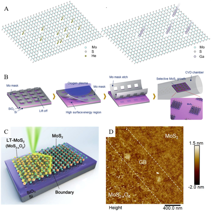
In recent years, with the progress of micro nano manufacturing technology, ion beam irradiation technology has been successfully used to control the density and size of defects in 2D materials [99]. Wang et al. successfully introduced high-density S vacancies and MoSn defects into single-layer MoS2 by using gallium ion and helium ion beam radiation [100]. Fig. 7A shows the schematic diagram of defects regulated by ion beam radiation. High magnification STEM images show that after He+ irradiation, S vacancies are mainly produced in single-layer MoS2, while after Ga+ irradiation, MoSn defects are mainly produced. It is worth noting that the MoS2 sample will have crack growth and Mo-S bond fracture in the process of ion beam radiation. More importantly, selective etching at the atomic level can be accomplished using ion-beam lithography, which can continuously adjust GB size and concentration within a specific range. At present, Sun et al. have successfully introduced high-density dislocations into monolayer MoS2 by using C+ ion beam irradiation, thereby improving its HER catalytic performance [101].
Figure 7
Figure 7.
(A) Schematic images of He+ and Ga+ irradiated suspended monolayer MoS2, as well as defects statistics. Reprinted with permission [100]. Copyright 2022, Wiley VCH. (B) Schematic outline of the MoS2 growth patterning procedure. Reprinted with permission [103]. Copyright 2017, Wiley VCH. (C) Schematic diagram of MoS2 and LT-MoS2 (MoS2−xOδ) junction fabricated via direct laser writing on a monolayer MoS2. The bottom-left region of the material is scanned by laser (LT-MoS2 or MoS2−xOδ), and the top-right region is unscanned and remains pristine (MoS2). The yellow line is used to highlight the GB between MoS2−xOδ and MoS2. (D) AFM image near the MoS2/MoS2−xOδ boundary. Reprinted with permission [105]. Copyright 2021, Wiley VCH.
To introduce GBs into TMDs in a controlled way, we can also conduct plasma treatment on the samples to be prepared. Nguyen et al. introduced high-density defects such as GBs through N2 plasma treatment of single-layer MoS2 film, and thus obtained a large number of active sites required for efficient HER performance [102]. The experimental results show that the defect density introduced is proportional to the time of plasma treatment. In addition to N2 plasma treatment, Kim et al. achieved the selective growth of MoS2 by using O2 plasma treatment [103]. Fig. 7B presents the whole process of oxygen plasma treatment. By using maskless lithography, Mo was entirely deposited on a SiO2/Si substrate. Next, oxygen plasma was employed for selective surface treatment. The MoS2 film is selectively formed by CVD after the Mo mask has been thoroughly etched with a wetting agent. By changing the growth conditions, such as the treatment duration, the treatment area size, and the nucleation site, it is possible to efficiently regulate the density of GBs and the grain size in MoS2. The grain size of MoS2 expanded along with its growth size, which led to a reduction in GB density. In addition, due to the high reactivity of GBs in the polycrystalline MoS2 film, Meng et al. clearly observed the separation of GBs in the sample after Ar plasma treatment [104]. Wang et al. successfully introduced GBs into single-layer MoS2 using direct laser writing technology [105]. Fig. 7C shows the schematic diagram of laser writing on single-layer MoS2 grown by CVD in air. The MoS2 sample was mildly oxidized and GBs started to appear after being exposed to the medium intensity laser beam. AFM was used to describe it afterwards, and the picture shows that the GB in the MoS2/MoS2−Oδ junction can be clearly observed (Fig. 7D). Direct laser writing technology allows people to design the defect area of the sample according to their own ideas, and regulate the distribution of GBs.
4.
Properties
GBs have a complicated and wide-ranging impact on the electrical, mechanical, thermal, optical, and other aspects of 2D TMDs. The misorientation angles of GBs will significantly affect the electron transport ability and thermal conductivity of 2D TMD films, and the existence of GBs will weaken the mechanical properties of the films which are actually correlated with the GB density. Additionally, the strain field introduced by GBs also has some influence on the intensity of PL.
4.1
Electronic properties
It is well known that as a typical TMD material, the electronic band gap of molybdenum disulfide monolayer increases with decreasing interlayer thickness [106]. On this basis, Huang et al. found that the band gap tunability is also related to the distance from the GB and can reach 0.85 ± 0.05 eV under its control [107]. The STS spectrum indicates that the band gap of the monolayer MoS2 thin film decreases with increasing interlayer thickness. Fig. 8A shows the scanning tunneling microscope image of single-layer MoS2, in which the GB appears as a bright line. As shown in Figs. 8B–D, when VTip decreases, the GB gradually disappears, which indicates that the electronic properties have changed. As the schematic diagram of Fig. 8E demonstrated, the bandgap size remains unchanged (1.55 eV) without deep gap states for d < 0.6 nm, while the gap decreases markedly in the range of 0.6 nm < d ≤ 2.0 nm. In order to further explore the influence of GBs on electronic properties, they also drew a series of STS spectra on the GBs in single-layer MoS2 (Fig. 8F). It was found that with the positive increase of the distance from the GB, the band gap increased from 1.55 eV at 0 nm to 2.40 eV at 4 nm, and remained unchanged after 4 nm. When the distance increases inversely, the band gap also increases. This work provides a new possibility for preparing flexible electronic devices.
Figure 8
Figure 8.
Unexpected bandgap tunability at the GB. (A) Large-scale STM image shows a SL MoS2 island composed of two grains, where the GB appears as bright protrusions (75 × 75 nm2; VTip = 1.5 V). (B-D) Bias-dependent images recorded at the boundary region highlighted by a black rectangle in panel A (8 × 4 nm2; B, VTip = 1.2 V; C, VTip = 1.0 V; D, VTip = −0.5 V). The misorientation between the grains I and II is 18° as determined in panel C. (E) Schematic diagram shows the bandgap change at the GB. (F) dI/dV spectra recorded at the positions denoted by the triangles in panel D (set point: VTip = 1.0 V, ITip = 100 pA). The variation of the bandgap with distance from the boundary is quite pronounced. Reprinted with permission [107]. Copyright 2015, Springer.
In some previous studies, the issue of how the atomic structure of GBs in monolayer MoS2 affects the electron transport characteristics has not been solved, and there is some controversy. Recently, however, the electric transport in monolayer MoS2 has been found to be related to the misorientation angles of GBs by combining the measurement of the atomic defect structure with the first-principle calculation [108]. Fig. 9A shows the schematic of a typical carrier transport across the GB. By selecting appropriate electrodes, the functional relationship between the misorientation angle and the field effect mobility is tested on the terminal equipment shown in Fig. 9B. The GB is located at the place marked by the red polyline, and it is composed of a series of 5|7 dislocation cores, as shown in the inset diagram in Fig. 9C. The number of equipment tested and the field effect mobility were statistically distributed, and a good normal distribution was observed after taking the logarithm of the mobility (Fig. 9D). The subsequent statistical distributions of the misorientation angle and field effect mobility (Fig. 9E) show that although there are some abnormal points in the low angle data, the mobility between domains increases at 8°–20°. When the angle is increased to the range of 20°–60°, the field effect mobility is large, showing good electric transport characteristics.
Figure 9
Figure 9.
(A) Experimental schematic of carrier transport across a GB. (B) SEM image of a device sample on SiO2/Si wafer; scale bar, 3 mm. After device characterization, the device was transferred to a TEM grid; scale bar, 6 mm (left inset). Right inset: Optical micrograph of the device with pre-etch flake shape outlined; scale bar, 30 mm. (C) Electrical performance of the device in panel (B) with α = 19° Intra-domain regions always have a higher μFE and reduced RS when compared to inter-domain. (D) Statistical distribution of the intra- and inter-domain mobilities with μFE(inter) < 16 cm2 V−1 s−1 < μFE(intra). The intra-domain μFE displays a log-normal distribution (black line) with expectation value μFE = 44 cm2 V−1 s−1, as exemplified by ln(μFE) in the inset. (E) The a-dependent μFE(inter) (blue) for 10 different angles with μFE(intra) (total of 43 devices). Here, μFE(inter) increases from 9° to 20°, but saturates for α > 20° at μFE(inter) < 16 cm2 V−1 s−1. The 19° dislocation is of the ‘Down’-type, while the others are ‘Up’-type. Reprinted with permission [108]. Copyright 2016, Springer.
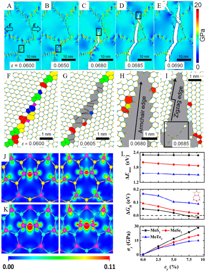
The mechanical properties of the pristine MoS2 flakes are relatively high and basically equivalent to those of stainless steel. However, it is still a difficult task to produce large area defect-free MoS2. The mechanical exfoliation method and the chemical exfoliation method are only limited to the production of small flakes of single-layer MoS2. Although the CVD method can produce large-area MoS2 with high yield, more nucleation sites on the substrate usually lead to polycrystalline microstructures connected by various GBs. The results of the mechanical experiment demonstrate that the bond of the polycrystalline structure at the GB is prone to brittle fracture and fracture initiation fractures because the higher the density of GBs in polycrystalline MoS2, the more likely it is that a stress concentration will develop. Therefore, the mechanical properties of MoS2 are significantly diminished by the presence of GBs [52]. Figs. 10A–I show the cracking of polycrystalline MoS2 under uniaxial tension. Cracks are generated at the GB after the stress is applied, and they will grow along the direction of the GB. When the crack grows to another GB, the growth direction will be deflected (Fig. 10C). It is worth mentioning that after the stress is applied, direct fracture of Mo-Mo bond and S-S bond occurs instead of dislocation migration (Figs. 10F and G). It is also observed that the cracks growing along the zigzag direction are sharper than those growing along the armchair direction (Figs. 10H and I), which demonstrate that polycrystalline MoS2 has relatively low zigzag edge energy. Moreover, the in-plane mechanical properties of polycrystalline MoS2 exhibit grain size-related traits, for polycrystalline MoS2 with grain size of micron, its mechanical strength is expected to be comparable to that of pristine MoS2.
Figure 10
Figure 10.
(A–E) Nucleation and propagation of both intergranular and transgranular cracks. Atoms in polycrystal are colored according to the values of von Mises stress. (F) Zoomed-in atomic configurations of one GB as marked by a black rectangle in panel a are highlighted. (G) Occurrence of dissociation of bonds in highlighted GB. Dash lines indicate the broken bonds. (H, I) Zoomed-in images of transgranular cracks along armchair and zigzag directions as marked by the black rectangles in panels c and d, respectively. Reprinted with permission [52]. Copyright 2018, American chemical society. (J) MoTe2 and (K) MoS2 under 0.0% (up) and 7.5% (down) uniaxial tensile strains. The Fermi level is set to be zero. The energy barriers ΔEmax of water molecules splitting on monolayer MoX2 in the presence of 22° Mo-rich 5|7 GBs (L), and the corresponding hydrogen adsorption free energies ΔGH after water dissociation and stress-strain curves under different y-direction uniaxial tensile strains εy. The inset shows the adsorption site of hydrogen. Reprinted with permission [109]. Copyright 2022, Springer.
Strain gradients generated by bending or wrinkling deformation in 2D TMDs result in remarkable out-of-plane charge polarization and flexoelectricity. The research of Pu et al. shows that when a single layer of TMD is subjected to in-plane tensile load, this non-uniform structural deformation will trigger the flexoelectric effect. It can be seen from Figs. 10J and K that the charge density at the Mo-Mo bond center and the charge polarization at the Mo atom are significantly enhanced when the uniaxial tensile strain is increased, which makes the binding ability of the Mo-Mo bond to the hydrogen atom stronger and reduces the free energy of hydrogen adsorption [109]. At the same time, we can see that compared with MoTe2, the charge density at the Mo-Mo bond center in MoS2 is larger, which also explains why the hydrogen adsorption free energy of single-layer MoS2 at its GB site is lower than that of MoTe2 when it also contains GBs. With the increase of y-axis tensile strain, the reaction energy barrier of monolayer MoS2 is slightly reduced under the premise that all contain 22° Mo-rich 5|7 GBs, while the free energy of hydrogen adsorption is especially decreased. The free energy of hydrogen adsorption of MoS2 is reduced to −0.005 eV when a 7.5% tensile strain is applied, exhibiting an excellent HER catalytic ability. With the same tensile strain applied, the stress of MoS2 is obviously higher than that of the other two materials (Fig. 10L). Overall, the flexural electrical effect induced by GBs under the action of tensile deformation effectively improved the catalytic properties of TMDs.
4.4
Thermal properties
Reports on the effect of GBs on thermal properties in 2D TMD materials are relatively limited. Sledzinska et al. conducted experiments on the thermal conductivity of polycrystalline MoS2 containing different grain sizes and orientations [110]. The experimental results show that the density of GBs between grains in the horizontal and vertical directions is the dominant factor in thermal conductivity. Molecular dynamics analysis and finite element simulation confirmed that the thermal conductivity increased with the proportion of vertically oriented grains. Xu et al. studied the influence of zigzag-oriented GB and armchair-oriented GB on thermal properties [111]. Figs. 11A–C show the relationship between the misorientation angle, linear tension, defect density and thermal resistance respectively. Mo5|7 and S5|7 GB in the figure belong to the armchair-oriented GB, which are represented in green and red respectively. Mo5|7 + S5|7 GB belongs to zigzag-oriented GB, which is indicated by yellow. Figs. 11B and C make it abundantly evident that as linear tension and GB density rise, so does the thermal resistance of both armchair- and zigzag-oriented GBs. However, when the misorientation angle increases, the thermal resistance of the zigzag-oriented GB rises while that of the armchair-oriented GB falls (Fig. 11A). In addition to grain orientation, the thermal conductivity of GBs formed by various dislocation centers varies. Compared with symmetric GBs, asymmetric GBs have lower defect concentrations and higher phonon-phonon scattering rate, which makes their thermal conductivity lower than that of symmetric GBs. The thermal conductivity of the armchair-oriented GBs, which are mainly made up of 4|8 dislocation cores, is the lowest, while the GBs formed by 4|6 dislocation cores have the highest thermal conductivity.
Figure 11
Figure 11.
Kapitza thermal resistance (R) of GBs in single-layer MoS2. (A–C) R of Mo5|7, S5|7 and Mo5|7 + S5|7 dislocation-dominated GBs in MoS2 bicrystals with length of 40, 75, and 120 nm of crystalline grain versus misorientation angle θ, line tension γ and defect density ρ, respectively. Reprinted with permission [111]. Copyright 2022, The Royal Society of Chemistry.
However, in general, the thermal conductivity of single-layer MoS2 grown by CVD is not significantly different from that of pristine MoS2, indicating that the GBs in single-layer MoS2 have a certain influence on the thermal conductivity, but not much. The impact of GBs on the thermal conductivity in TMDs still requires additional research due to the dearth of pertinent literature.
4.5
Optical properties
Monomolecular TMDs are widely used in various devices, and their structural stability is closely related to the surrounding environment. Cai et al. characterized the thermal stability of WS2 prepared by CVD through the PL intensity of GBs [112]. According to the experimental findings, the PL intensity of GB region in single-layer WS2 is less thermally stable than the non-GB region, which suggests that the PL intensity of GB region is more temperature-sensitive. The luminous intensity of the GB zone rises together with the temperature, and the PL intensity of the sample likewise starts to decrease when it is heated to the point of disappearance.
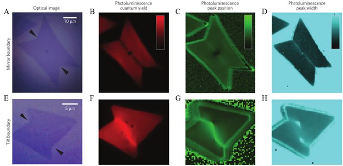
Notably, both an increase and a decrease in PL intensity were observed at the GB simultaneously [68]. Figs. 12A and E are optical images of mirror boundary and inclined boundary in MoS2 samples prepared by CVD, where GBs cannot be quickly and effectively identified. Figs. 12B–D and F–H show the maps of PL intensity, peak position and peak width. We can observe that a series of PL changes occur at the GBs. The brightness at the mirror boundary is low, and the PL intensity is quenched by approximately 50%. However, the tilt boundary shows a bright curve, and the PL intensity is enhanced by about 100%. This phenomenon may be brought on by the doping and strain at GBs, and is related to misorientation angles [113-115].
Figure 12
Figure 12.
Optical properties of mirror and tilt boundaries. (A-D) Optical measurements of an island containing a mirror twin boundary. (E–H) Corresponding measurements for an island containing a tilt boundary. (A) and (E) are optical images. (B-D) and (F-H) are color plots of photoluminescence. In (B) and (F), red is the relative quantum yield, with color scale 0–1100 a.u. We see 50% quenching at the mirror twin boundary and a 100% enhancement at the tilt boundary. In (C) and (G), green is the peak position, with color scale 1.82–1.87 eV. There is an upshift of 8 meV at the mirror twin boundary, and a much stronger 26 meV upshift in the tilt boundary. In (D) and (H), cyan is the peak width with color scale of 53–65 meV. The peak broadens from 55 meV to 62 meV at the boundary in both samples. Reprinted with permission [68]. Copyright 2013, Springer.
At present, atom-thin TMDs have become an important material and key structure in the field of electrocatalysis [116-118]. To date, their edges, dopant heteroatoms and defects have been widely explored as active sites for HER to split water [119-121]. However, as a key defect type in TMDs, GBs are often ignored in the above-mentioned problems due to their low density and large structural changes. Experiments show that the basal plane of MoS2 is quite inert, so it is generally believed that the catalytic activity comes from its edge and various technologies such as interface electronic coupling and phase engineering have been developed to remove the limitation of basal plane in the practical application of HER [122].
5.1
Theoretical research
First-principles calculations are utilized to estimate their HER activity in order to further assess the impact of GBs and dislocations in TMDs on their HER catalytic performance. Calculations can help to clarify the HER catalytic performance of TMDs, which can offer theoretical direction for the preparation of efficient HER catalysts. Ouyang et al. conducted atomic modeling for defects such as GBs and dislocations in single-layer MoS2 nanosheets, and systematically evaluated their ability to affect MoS2 catalytic activity [123]. Fig. 13A shows the most stable adsorption configuration of a single H atom in all point defects and GB regions, and the GB structure model dominated by 5|7 dislocations was established by inserting a nanosheet with the same structure but different orientations between two identical MoS2 nanosheets. It can be seen from Figs. 13B and C that the free energy of hydrogen adsorption of 4|8a and Mo-Mo bond GBs is low, which is close to that of Pt catalyst. Additionally, the Tafel slope of 4|8a GB is quite low, indicating remarkable activity in Tafel reaction. The above calculated data show that defect structures such as GBs and dislocations in single-layer MoS2 have a strong ability to activate the basal plane, which can increase the amount of catalytic sites and significantly enhance the HER catalytic performance of MoS2. Therefore, it is anticipated to replace Pt and other noble metal catalysts in HER by regulating the GBs in 2D TMD materials.
Figure 13
Figure 13.
(A) The most stable adsorption positions for singe H atom absorbing at VS, VS2, VMoS3, VMoS6, MoS2, MoS, Mo2S2, S2Mo, SMo PDs and 5|7a, 5|7b, 4|8a, 4|8b, Mo-Mo bond, S bridge, 4|4 GBs. The yellow, purple and cyan balls refer to the S, Mo, and H atoms in defect regions, respectively. Defect regions are colored and framed by the dash line. (B) Energetics of the HER process on different catalysts: 5|7a, 5|7b, 4|8a, 4|8b, Mo-Mo bond, S bridge, 4|4 GBs and Pt. (C) Energetics of HER process on different catalysts: VS, VS2, VMoS3, VMoS6, MoS2, MoS, Mo2S2, S2Mo, SMo PDs and Pt. Reprinted with permission [123]. Copyright 2016, American chemical society.
Apparently, in addition to theoretical calculations, engineering the density and structure of GB in 2D TMD films have a pronounced impact on the performance of the catalyst. At present, MoS2, as a promising HER catalyst, its performance is largely limited by the low density of active sites in the basal plane [124,125]. Although it can be improved by introducing S vacancies, the vacancy defects in MoS2 can easily cause instability of its surface. To fully develop the potential of MoS2 in HER, Zhu et al. developed a systematic method to activate monolayer MoS2 bases via introducing 2H-2H domain boundaries and 2H-1T-phase boundaries, which were able to provide ultra-high density of active sites and maintain surface stability at the same time [126]. Figs. 14A–C show three different types of MoS2 samples for experiments, in which type-Ⅰ does not contain a 2H-2H domain boundary, type-Ⅱ has a low density of 2H-2H domain boundaries, and type-Ⅲ contains a high density of 2H-2H domain boundaries. After comparing the HER polarization curve and Tafel slope, it is found that the catalytic performance of type-Ⅲ sample is significantly better than that of type-Ⅰ sample, which indicates that 2H-2H domain boundaries can play a role in enhancing the HER activity. In addition, the 2H-1T-phase boundaries can also be used as active sites in HER. Fig. 14D shows the schematic diagram of the MoS2 catalyst used for electro catalytic HER test, and the 2H-1T-phase boundaries can be formed by plasma bombardment on the pristine sample. It can be vividly shown from Fig. 14E that 2H-1T-phase boundary has better HER activity, and a higher boundary density also exhibits better performance after prolonging the treatment time. Moreover, due to the stability of 2H-2H and 2H-1T boundary structures, the catalyst exhibits exceptional security (Fig. 14F). Considering that the phase boundary and domain boundary are actually GBs composed of different dislocation cores, this experiment further proved the importance of GBs and dislocations in regulating the HER catalytic performance of MoS2.
Figure 14
Figure 14.
(A) Optical image of the type-Ⅰ MoS2 with individual domain size of few hundreds microns transferred onto a TEM grid. (B) HRTEM images of as-grown type-Ⅱ MoS2 film with highly orientated domains of few microns for the domain sizes. (C) False-color dark-field TEM image of type-Ⅲ MoS2 with high-density 2H–2H domain boundaries. (D) Schematic structure of the multi-hierarchy MoS2 catalysts with both high density of domain and phase boundaries. (E) Polarization curves for pristine type-Ⅱ samples, pristine type-Ⅲ samples, a series of heterophase type-Ⅲ samples with different phase boundary densities and Pt. (F) Time-dependent current density curve for a multi-hierarchy MoS2 catalyst under static overpotential of 150 mV for 200 h. Reprinted with permission [126]. Copyright 2019, Springer. (G) Schematic of the micro-electrochemical cell for HER measurements, where graphene serves as a vertical electron injector. (H) Polarization curves of the current density and (I) the corresponding Tafel plots of the MoS2 devices. The window size is ~80 µm2 for each device. Reprinted with permission [93]. Copyright 2020, Springer.
In addition to the design of GBs in single-layer MoS2, the introduction of high-density GB defects can also activate its inert basal plane, thereby improving the inherent hydrogen evolution activity of MoS2. He et al. successfully prepared single-layer MoS2 nanofilms with an ultra-high density of GBs using the improved CVD method under 2D limit, which can be explained by a climb and drive 0D/2D-interaction-based growth mechanism [93]. Subsequently, a micro electrochemical cell was developed to explore the HER activity of the film, and its schematic diagram is shown in Fig. 14G. The polarization curve and the corresponding Tafel slope in acidic solution environment were characterized through tests (Figs. 14H and I). We can see intuitively from the figure that the MoS2 nanofilm shows excellent HER catalytic performance: −25 mV starting potential and 54 mV/dec Tafel slope. Although there is still a gap between this and the performance of Pt based catalysts, it is sufficient to demonstrate that the possibility of replacing Pt with MoS2 based catalysts is further increased by introducing high-density GB defects.
The introduction of a significant number of GBs and dislocations in TMDs is often accompanied by strain effects, which will change the electronic structure at defects. Wang et al. studied the relationship between the stress field introduced by dislocations and the HER catalytic performance of MoS2 [94]. On the one hand, a large number of dislocation defects can not only act as active sites to activate the inert basal plane of MoS2, but also make the surface of the catalyst bulge or sag, thus increasing the specific surface area of the catalyst. On the other hand, the local strain introduced by dislocation defects regulates the electronic structure of the active site, making the free energy of hydrogen adsorption close to zero.
As a powerful tool to determine the relationship between the surface morphology of the sample and its electrochemical activity, the scanning electrochemical microscope can quantitatively evaluate the relationship between the catalytic activity and the spatial resolution, and has been used to screen the highly catalytic active sites in TMDs. Takahashi et al. used high-resolution scanning electrochemical cell microscopy to investigate the HER catalytic activity sites of 1H-MoS2 nanosheets. The scanning electrochemical cell microscopy was equipped with a scanning nanopipette probe for detection in local and mobile electrochemical cells, and after measuring at all scanning points, it provided three electrochemical mapping images of HER current, Tafel slope, and overpotential. These results revealed that HER activity at GBs in MoS2 nanosheets is not homogeneous and that GB engineering can enhance the HER catalytic performance of MoS2 nanosheets [127]. By examining the current noise from electrochemical scanning tunneling microscopy, Lunardon et al. investigated the catalytic activity of monolayer MoSe2 films in HER and confirmed that defects, including GBs, are extremely stable and have modest activity [128].
6.
Conclusions and outlook
In summary, GBs have a significant impact on the functionality and properties of 2D TMDs, involving electronic, thermal, optical, chemical, catalytic and other fields. As a kind of defect, although the existence of GBs may have some adverse effects on the performance of materials and devices, their unique properties can open up some potential applications in devices. Through some previous studies, we know that the structure, properties, preparation, characterization and application of 2D TMDs have formed a relatively systematic framework, but research on GBs is still in its infancy and faces some flaws and challenges. Herein, we sorted out our outlook as follows.
(1) The introduction of GBs with controllable density and type is the premise for their good application in transistors, memristors, optoelectronic devices and flexible electronic devices. At present, only CVD can prepare polycrystalline TMD films with uniform properties on a large scale. Although other preparation methods can also introduce GBs into 2D TMDs, it is impossible to obtain large-scale application in industry due to the limitation of growth conditions. Therefore, it is still necessary to develop a large-scale and easily controlled synthesis method that can introduce GBs.
(2) To fully understand the GB structure in 2D TMDs, we need to quickly and effectively visualize it. Generally, TEM and other electron microscopes can provide detailed information on the GB structure, but their disadvantages are time-consuming, small characterization area and the need to use some special substrates. Of course, the use of methods such as water vapor etching and ultraviolet radiation can play a good auxiliary role, but it also easily causes damage to the GB area. In addition, PL mapping has the disadvantage of being time-consuming, which is difficult to apply to the characterization of large-area samples. Although the optical microscope provides high sensitivity and a fast response time, the rotation angle between adjacent crystal structures relative to the crystal axis has a certain impact on the final imaging. Therefore, it is still a challenge to develop a fast, effective, in situ and non-invasive characterization method.
(3) We note that the GBs in 2D TMDs provide the possibility to develop new applications and improve the performance of devices based on TMDs. For example, GBs can be used as favorable active sites for ion adsorption in WS2-based gas sensors, and can also be used as gate-tunable heterosynaptic functionality mimicking neurons in MoS2-based memristors. However, in general, although GBs are predicted to have the ability to improve the performance of devices, related applications are still deficient.
(4) Although the atomic structure of the GBs in 2D TMDs has been relatively well studied, there are still some unsolved problems about how the GBs and the dislocation cores change the properties of 2D TMDs. These problems need further theoretical and experimental research.
In general, it is a promising method to further improve the performance of 2D TMDs through GBs. We sincerely hope that this review can provide some help for the application of GBs and the development of TMDs.
Declaration of competing interest
The authors declare that they have no known competing financial interests or personal relationships that could have appeared to influence the work reported in this paper.
Acknowledgments
This work was financially supported by the Natural Science Foundation of China (No. 51902101), Natural Science Foundation of Jiangsu Province (No. BK20201381), Science Foundation of Nanjing University of Posts and Telecommunications (No. NY219144) and the National College Student Innovation and Entrepreneurship Training Program (No. 202210293171K).
[1]
S. Najmaei, Z. Liu, W. Zhou, et al., Nat. Mater. 12 (2013) 754–759. doi: 10.1038/nmat3673
[2]
T. Taniguchi, L. Nurdiwijayanto, S. Li, et al., ACS Nano 14 (2020) 6663–6672. doi: 10.1021/acsnano.9b09253
[3]
X. Yin, Z. Ye, D.A. Chenet, et al., Science 344 (2014) 488–490. doi: 10.1126/science.1250564
Y. Takahashi, Y. Kobayashi, Z. Wang, et al., Angew. Chem. Int. Ed. 59 (2020) 3601–3608. doi: 10.1002/anie.201912863
[128]
M. Lunardon, T. Kosmala, M. Ghorbani-Asl, et al., ACS Energy Lett. 8 (2023) 972–980. doi: 10.1021/acsenergylett.2c02599
Figure 1
Grains and GB structures in 2D polycrystalline MoS2. (A) Typical loop and (B) Y-shaped GBs captured from the polycrystal. The black arrows indicate the zigzag direction of bulk of grain. Boundary misorientation angles are explained by the angles between the arrow vectors in the neighboring grains. GBs are composed of diverse dislocation cores, depending on boundary misorientation angles. The right side shows typical dislocation cores captured from GBs in polycrystal, and they are individually named according to the feature of ring pairs for clarification. Reprinted with permission [52]. Copyright 2018, American Chemical Society.
Figure 2
(A) MoS2 film with S4|6 and S6|8 GBs. (B) Migration process of S4|6 GB. (C) Migration process of S6|8 GB. The different GBs are filled with different colors. Reprinted with permission [53]. Copyright 2020, The Royal Society of Chemistry.
Figure 3
(A) Optical image with marked grains (A1, A2, B1 and B2) and GBs (GB1, GB2, GB3 and GB4). (B) Experimental SHG image without analyser. (C) Experimental THG image without analyser. Reprinted with permission [63]. Copyright 2017, Springer. (D) Schematic illustration of the thermal treatment that enabled direct imaging of WS2 GBs using an optical microscope. (E, F) Optical images of WS2 GBs in other monolayer configurations of the as-formed WS2 crystal. Reprinted with permission [64]. Copyright 2015, American Chemical Society. (G–I) Dark-field optical images of MoS2, WS2, and WSe2. Scale bar is 20 µm. Reprinted with permission [65]. Copyright 2015, American Chemical Society.
Figure 4
(A) Schematic diagram for UV treatment monolayer WSe2. (B, C) AFM and SEM image of pristine WSe2. (D, E) AFM and SEM image of oxidized WSe2 after 6 min UV treatment. Reprinted with permission [66]. Copyright 2014, American Chemical Society. (F) In the large-scale STM image, the 6° GB is meandering and aperiodic (100 × 100 nm2; scale bar, 10 nm; Vtip = −1.2 V), where the insets (i) and (ii) reveal the different lattice orientations for the corresponding domains (each inset: 3 × 3 nm2; scale bar, 1 nm; Vtip = 0.6 V). (G) Another aperiodic GB with a misorientation angle of 3° (60 × 60 nm2; scale bar, 10 nm; Vtip = −1.0 V). Reprinted with permission [67]. Copyright 2016, American Chemical Society. (H) High-resolution ADF-STEM image of a mirror twin boundary. The boundary is visible just below the annotated line. The annotation indicates the nanoscale faceting of the boundary at ±20° off the zigzag direction. (I) Zoomed-in image of the GB shows a periodic line of 8-4-4 ring defects. (J) An atomistic model of the experimental structure shown in (I). Reprinted with permission [68]. Copyright 2013, Springer.
Figure 5
PL characterization of polycrystalline MoS2 star with twin GBs. (A) Optical image of a MoS2 star sitting on SiO2. (B) PL intensity mapping. The edges and twin GBs have a higher intensity (light yellow), while rest are depicted in orange. (C) PL peak position mapping. PL spectra are collected at the location marked five dots with different colours. Scale bar: 3 µm. (D) PL spectra collected from points indicated in (C). Each spectrum corresponds to the location in (C) with the same color. (E, F) PL intensity and peak position line profiles as indicated by the white dash lines crossing two GBs and two edges. Reprinted with permission [70]. Copyright 2014, Springer.
Figure 6
(A) Schematic of the wafer-scale growth of TMD nanograin films. Ultra-high-density Au quantum dots (QDs) were used to grow the MoS2 (as well as WS2 atom-thin films: see Supporting information). Reprinted with permission [93]. Copyright 2020, Springer. (B) Schematic diagram of synthetic high-density dislocation intrinsic flexible MoS2 nanosheets. Reprinted with permission [94]. Copyright 2022, Springer. (C) Schematic of a conventional PLD setup. Reprinted with permission [96]. Copyright 2021, Elsevier. (D) High-resolution ADF STEM image of a 180° twin GB showing a periodic line of defects with 4|8 motif rings. The overlaid triangles denote the twin grains rotated by 180° with respect to each other. (E) Simulated STEM image of a GB relaxed structure reproducing the 4|8 structure. The yellow scale bar has a length of 5 Å. Reprinted with permission [97]. Copyright 2021, American Chemical Society.
Figure 7
(A) Schematic images of He+ and Ga+ irradiated suspended monolayer MoS2, as well as defects statistics. Reprinted with permission [100]. Copyright 2022, Wiley VCH. (B) Schematic outline of the MoS2 growth patterning procedure. Reprinted with permission [103]. Copyright 2017, Wiley VCH. (C) Schematic diagram of MoS2 and LT-MoS2 (MoS2−xOδ) junction fabricated via direct laser writing on a monolayer MoS2. The bottom-left region of the material is scanned by laser (LT-MoS2 or MoS2−xOδ), and the top-right region is unscanned and remains pristine (MoS2). The yellow line is used to highlight the GB between MoS2−xOδ and MoS2. (D) AFM image near the MoS2/MoS2−xOδ boundary. Reprinted with permission [105]. Copyright 2021, Wiley VCH.
Figure 8
Unexpected bandgap tunability at the GB. (A) Large-scale STM image shows a SL MoS2 island composed of two grains, where the GB appears as bright protrusions (75 × 75 nm2; VTip = 1.5 V). (B-D) Bias-dependent images recorded at the boundary region highlighted by a black rectangle in panel A (8 × 4 nm2; B, VTip = 1.2 V; C, VTip = 1.0 V; D, VTip = −0.5 V). The misorientation between the grains I and II is 18° as determined in panel C. (E) Schematic diagram shows the bandgap change at the GB. (F) dI/dV spectra recorded at the positions denoted by the triangles in panel D (set point: VTip = 1.0 V, ITip = 100 pA). The variation of the bandgap with distance from the boundary is quite pronounced. Reprinted with permission [107]. Copyright 2015, Springer.
Figure 9
(A) Experimental schematic of carrier transport across a GB. (B) SEM image of a device sample on SiO2/Si wafer; scale bar, 3 mm. After device characterization, the device was transferred to a TEM grid; scale bar, 6 mm (left inset). Right inset: Optical micrograph of the device with pre-etch flake shape outlined; scale bar, 30 mm. (C) Electrical performance of the device in panel (B) with α = 19° Intra-domain regions always have a higher μFE and reduced RS when compared to inter-domain. (D) Statistical distribution of the intra- and inter-domain mobilities with μFE(inter) < 16 cm2 V−1 s−1 < μFE(intra). The intra-domain μFE displays a log-normal distribution (black line) with expectation value μFE = 44 cm2 V−1 s−1, as exemplified by ln(μFE) in the inset. (E) The a-dependent μFE(inter) (blue) for 10 different angles with μFE(intra) (total of 43 devices). Here, μFE(inter) increases from 9° to 20°, but saturates for α > 20° at μFE(inter) < 16 cm2 V−1 s−1. The 19° dislocation is of the ‘Down’-type, while the others are ‘Up’-type. Reprinted with permission [108]. Copyright 2016, Springer.
Figure 10
(A–E) Nucleation and propagation of both intergranular and transgranular cracks. Atoms in polycrystal are colored according to the values of von Mises stress. (F) Zoomed-in atomic configurations of one GB as marked by a black rectangle in panel a are highlighted. (G) Occurrence of dissociation of bonds in highlighted GB. Dash lines indicate the broken bonds. (H, I) Zoomed-in images of transgranular cracks along armchair and zigzag directions as marked by the black rectangles in panels c and d, respectively. Reprinted with permission [52]. Copyright 2018, American chemical society. (J) MoTe2 and (K) MoS2 under 0.0% (up) and 7.5% (down) uniaxial tensile strains. The Fermi level is set to be zero. The energy barriers ΔEmax of water molecules splitting on monolayer MoX2 in the presence of 22° Mo-rich 5|7 GBs (L), and the corresponding hydrogen adsorption free energies ΔGH after water dissociation and stress-strain curves under different y-direction uniaxial tensile strains εy. The inset shows the adsorption site of hydrogen. Reprinted with permission [109]. Copyright 2022, Springer.
Figure 11
Kapitza thermal resistance (R) of GBs in single-layer MoS2. (A–C) R of Mo5|7, S5|7 and Mo5|7 + S5|7 dislocation-dominated GBs in MoS2 bicrystals with length of 40, 75, and 120 nm of crystalline grain versus misorientation angle θ, line tension γ and defect density ρ, respectively. Reprinted with permission [111]. Copyright 2022, The Royal Society of Chemistry.
Figure 12
Optical properties of mirror and tilt boundaries. (A-D) Optical measurements of an island containing a mirror twin boundary. (E–H) Corresponding measurements for an island containing a tilt boundary. (A) and (E) are optical images. (B-D) and (F-H) are color plots of photoluminescence. In (B) and (F), red is the relative quantum yield, with color scale 0–1100 a.u. We see 50% quenching at the mirror twin boundary and a 100% enhancement at the tilt boundary. In (C) and (G), green is the peak position, with color scale 1.82–1.87 eV. There is an upshift of 8 meV at the mirror twin boundary, and a much stronger 26 meV upshift in the tilt boundary. In (D) and (H), cyan is the peak width with color scale of 53–65 meV. The peak broadens from 55 meV to 62 meV at the boundary in both samples. Reprinted with permission [68]. Copyright 2013, Springer.
Figure 13
(A) The most stable adsorption positions for singe H atom absorbing at VS, VS2, VMoS3, VMoS6, MoS2, MoS, Mo2S2, S2Mo, SMo PDs and 5|7a, 5|7b, 4|8a, 4|8b, Mo-Mo bond, S bridge, 4|4 GBs. The yellow, purple and cyan balls refer to the S, Mo, and H atoms in defect regions, respectively. Defect regions are colored and framed by the dash line. (B) Energetics of the HER process on different catalysts: 5|7a, 5|7b, 4|8a, 4|8b, Mo-Mo bond, S bridge, 4|4 GBs and Pt. (C) Energetics of HER process on different catalysts: VS, VS2, VMoS3, VMoS6, MoS2, MoS, Mo2S2, S2Mo, SMo PDs and Pt. Reprinted with permission [123]. Copyright 2016, American chemical society.
Figure 14
(A) Optical image of the type-Ⅰ MoS2 with individual domain size of few hundreds microns transferred onto a TEM grid. (B) HRTEM images of as-grown type-Ⅱ MoS2 film with highly orientated domains of few microns for the domain sizes. (C) False-color dark-field TEM image of type-Ⅲ MoS2 with high-density 2H–2H domain boundaries. (D) Schematic structure of the multi-hierarchy MoS2 catalysts with both high density of domain and phase boundaries. (E) Polarization curves for pristine type-Ⅱ samples, pristine type-Ⅲ samples, a series of heterophase type-Ⅲ samples with different phase boundary densities and Pt. (F) Time-dependent current density curve for a multi-hierarchy MoS2 catalyst under static overpotential of 150 mV for 200 h. Reprinted with permission [126]. Copyright 2019, Springer. (G) Schematic of the micro-electrochemical cell for HER measurements, where graphene serves as a vertical electron injector. (H) Polarization curves of the current density and (I) the corresponding Tafel plots of the MoS2 devices. The window size is ~80 µm2 for each device. Reprinted with permission [93]. Copyright 2020, Springer.

 DownLoad:


 下载:
下载:


