School of Material Science and Engineering, Shaanxi University of Science and Technology, Xi'an 710021, China
b.
Center of Nanomaterials for Renewable Energy (CNRE), School of Electrical Engineering, Xi'an Jiaotong University, Xi'an 710049, China
c.
Institute of Environmental and Energy Catalysis, School of Materials Science and Chemical Engineering, Xi'an Technological University, Xi'an 710021, China
Received Date:
13 September 2022 Accepted Date:
07 February 2023 Revised Date:
20 January 2023 Available Online:
15 September 2023
Abstract:
Two dimensional (2D) materials are promising gas sensing materials, but the most of them need to be heated to show promising sensing performance. Sensing structures with high sensing performance at room-temperature are urgent. Here, another 2D material, violet phosphorus (VP) nanoflake is investigated as gas sensing material. The VP nanoflakes have been effectively ablated to have layers of 1–5 layers by laser ablation in glycol. The VP nanoflakes are combined with graphene to form VP/G heterostructures-based NO sensor. An ultra-high gauge factor of 3 × 10⁷ for ppb-level sensing and high resistance response of 59.21% with ultra-short recovery time of 6s for ppm-level sensing have been obtained. The sensing mechanism is also analysed by density functional theory (DFT) calculations. The adsorption energy of VP/G is calculated to be −0.788 eV, resulting in electrons migration from P to N to form a P−N bond in the gap between VP and graphene sheet. This work provides a facile approach to ablate VP for mass production. The as-produced structures have also provided potential gas sensors with ultrasensitive performance as ppb-level room-temperature sensors.
Gas sensors are one of important approach to rapidly detect the diseases from the expired gas of patients. amongst them, NO gas is the most comment gas from lung disease. The traditional gas sensitive materials [1-3] no longer meet the increasingly needs of our daily life. Active sites [4] and active structures [5] are two main approaches to improve gas sensors. 2D materials have attracted numerous attentions for gas sensing due to the ultra-high specific surface area and abundant active sites. The graphene-based sensors have been widely studied to detect different harmful gases [6-8]. The black phosphorus (BP) is also used as gas sensor due to the lone pare electrons of phosphorus [9]. A BP nanometre steam sensor [10] was developed for detecting hydrogen peroxide (H2O2) to have a detection limit of 1 × 10⁻⁷ mol/L. The BP nanometers doped with Pt nanoparticles had high hydrogen sensing [11]. However, BP were unstable at ambient conditions. Whereas, violet phosphorus (VP) was the most stable phosphorus allotropes in 2019 [12]. The researches of VP have been mainly focusing on its intrinsic characteristics, such as electronic structure [13], work function [14], mechanical property [15,16], phonon property [17], and anisotropy [18]. The application of VP as gas sensing has not involved yet. The unique electronic structure with lone pair electrons of VP [12] provides natural active sites as superb candidate for gas sensing. Up to date, the ppb-level gas sensing is far from practical application, and most of the gas sensing materials were performed at the temperature higher than 100 ℃, even 200–300 ℃. Room-temperature ppb-level sensors are urgent for real-life applications. Additionally, aggregation of materials, degeneration of structures, or surface inhomogeneity, still remain to be solved. Herein, VP nanoflakes have been investigated as gas sensing materials. A feasible approach has been approached to yield VP nanoflakes for gas sensing by laser ablation. The VP nanoflakes were filtered onto graphene to form VP/G heterostructures for gas sensing. This work provides a new perspective to design sensing materials for industrialization of nanomaterials, and further enriches the options of high-quality gas sensors.
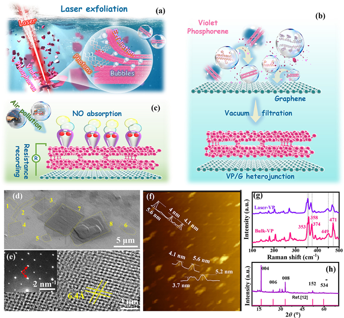
The experiments are overviewed in Figs. 1a and c and the details are presented in Supporting information. The original bulk VP was prepared by a chemical vapour transport. Then, the laser was applied to ablated the bulk VP to VP nanoflakes (Fig. 1a). The VP nanoflakes were combined with graphene to form a VP/G heterojunction structure on PES membrane (Fig. 1b). The gas sensing tests were implemented on a self-built vacuum probe platform. The testing gas was NO and CO with the concentration from 50 ppb to 500 ppm. The apparatuses are presented in Fig. S1 (Supporting information). The real-time resistance was record to evaluate the sensitivity of as-produced VP/G sensors (Fig. 1c and Fig. S1c). Density functional theory (DFT) calculations were applied for analyses the sensing mechanism, and the set-up details were described in Supporting information.
Figure 1
Figure 1.
Process flow diagram: (a) Laser ablation of VP, (b) VP/G heterojunction. (c) Sensing performance test. Topography and structure of VP after laser ablation: (d) SEM image, (e) HRTEM image and SAED in the inset, (f) AFM image, (g) Raman spectrum, and (h) XRD spectrum.
The topography and structure of VP nanoflakes after laser ablation are shown in Figs. 1d-h, under the optimal conditions: spot diameter of 50 µm, laser power of 60 W, scanning speed of 10 mm/s, scanning times of 15. The layered structure is observed by scanning electron microscopy (SEM) and transmission electron microscopy (TEM) image (Fig. 1d, and Figs. S2a-c in Supporting information). Two set of orthogonal crystal planes with the interplanar spacing of 6.4 Å corresponding to (110) and (110) planes of VP are shown in Fig. 1e. The selected area electron diffraction (SAED) pattern further indicates the zone axis of (001). A high crystallinity has been demonstrated by the clear lattice fringe and sharp SAED patterns (Fig. 1e, Fig. S2c). The height profile of the exfoliated VP nanoflakes in Fig. 1f were measured by atomic force microscopy (AFM) to be 4.26 nm (average from the random locations in Figs. S2d-k in Supporting information), corresponding to 4 layers. The Raman (Fig. 1g) and XRD (Fig. 1h) features are well in accord with the Ref. [12,19], demonstrating the feasibility of laser ablation to fabricate VP nanoflakes.
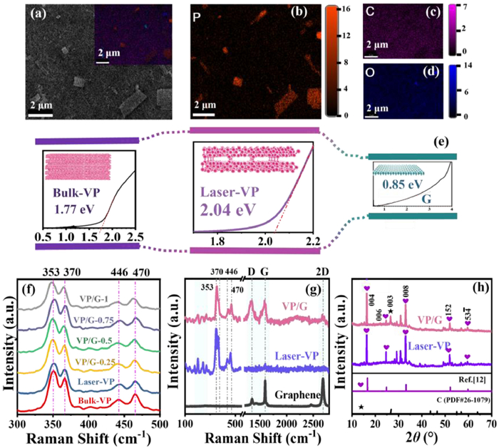
The VP nanoflakes were tiled on graphene films to form heterojunction as gas sensors [20,21]. The graphene was 5–7 layers, characterized by Raman and TEM (Fig. S3 in Supporting information). The VP nanoflakes were observed to have rectangular shapes and well titled on graphene (Fig. 2a). The rectangular VP nanoflakes were confirmed by elemental mapping analysis to contain phosphorus, where small amount of oxygen was observed on surface (Figs. 2b–d). The surface oxygen was removed by heating treatment (100 ℃, 2 h) before sensing tests. The bottom graphene surface was also observed by the elemental mapping analysis (Fig. 2c). The bandgap of bulk VP and VP nanoflakes were measured by ultraviolet-visible (UV-vis) spectrophotometer to be 1.77 and 2.04 eV, respectively (Fig. 2e, Fig. S4 in Supporting information), well consistent with reported data [12]. The bandgap of graphene was measured to be 0.85 eV. Combined with the graphene, the mobility of VP can be improved, and the charge can migrate from graphene to VP to form the heterojunction. Raman spectra (Fig. 2f) show the structure of bulk VP, laser-ablated VP, and VP/G with different amount of VP (0.25 to 1 mg). Raman spectra of bulk VP and laser-ablated VP are fairly similar, demonstrating that the laser process just reduced the size of bulk VP to nanoflakes, rather than changed the intrinsic structure of VP. After being combined with graphene, the characteristic peaks (353, 370, 446, and 470 cm−1) of VP/G generates bathochromic shift. The degree of bathochromic shift is enhanced with the VP amounts increasing. The bathochromic shift reveals lengthening of P−P bonds and weakening of lattice vibration, leading to lower electron concentration and lower Fermi energy [20]. The charge carriers can migrate from graphene to VP, and then VP/G heterojunction can be formed. The typical peaks (D, G and 2D) of graphene are observed during the 1000–2800 cm−1 in Fig. 2g, showing the successful combination of VP and graphene by the coupling between the π conjugate electron orbit of graphene and the abandon lone pair electrons of VP [22]. The graphene signal (2θ = 26.54°) is also observed in XRD spectrum in Fig. 2h, marked by star (003), demonstrating the hybrid of graphene and VP. The interaction is further identified by sheet resistance of VP/G (Fig. S5 in Supporting information). The sheet resistance of pure graphene is ultra-low (0.3 kΩ) and that of pure VP is ultra-high (4706 kΩ). For VP/G, the sheet resistance (1.3 kΩ) is much lower than that of pure VP, but higher than that of pure graphene. It presents that the charge carriers are supplied from graphene to VP, forming VP/G heterojunction.
Figure 2
Figure 2.
Topography and structure of VP/G heterojunction. (a) SEM image with EDS mapping in the inset: (b) P distribution, (c) C distribution, (d) O distribution. (e) Band gap of bulk violet phosphorus, VP and graphene. (f) Raman spectra in 300–500 cm−1. (g) Raman spectra in 100–2800 cm−1. (h) XRD spectra of VP and VP/G.
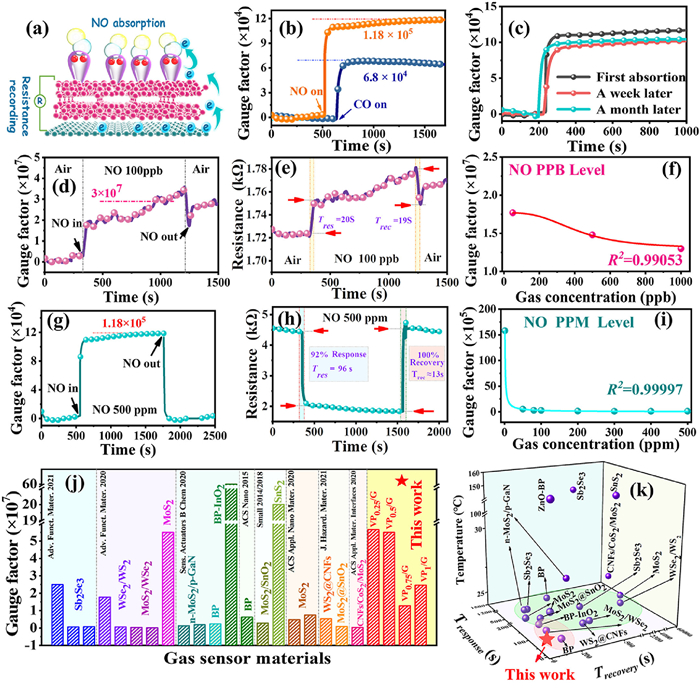
Sensitivity (defined as gauge factor, Eq. S1 in Supporting information) and resistance response (Eq. S2 in Supporting information) are the critical indexes to evaluate the quality of sensors. The resistance of the VP/G has varied since the adsorption of gas molecules, inducing the transfer of electron (Fig. 3a). NO and CO gas were applied to investigate the VP/G sensing performance. The gauge factor of VP/G to CO gas is 6.8 × 10⁴ (Fig. 3b), much lower than that of NO sensing. The sensing selectivity (NO/CO) reaches up to 1.7, giving high sensitivity and selectivity of VP/G heterojunction in sensing NO. The VP/G sensor was also demonstrated to have a high stability. The sensing response of VP/G sensor was still measured to be 52.26% after one month (Fig. 3c), which is more than 89% of its original value of 59.21%. For ppb-level sensing, the room-temperature gauge factor is up to 3.0 × 10⁷ (Fig. 3d). Notably, the response time and recovery are ultra-fast, only taking 20 s to respond and 19 s to recover to the initial resistance (Fig. 3e). The fitting of gauge factor in Fig. 3f shows that the gauge factor would be higher in several ppb, revealing much low limit of detection. For ppm-level sensing, the gauge factor of VP/G is 1.18 × 10⁵ (Fig. 3g), and the corresponding resistance response is 59.21%, taking 13 s to recover to the initial resistance (Fig. 3h). The fitting of gauge factor for ppm sensing shows the stable of the sensing performance in Fig. 3i, independent from NO concentration. Compared to pure VP and pure graphene (Fig. S6 in Supporting information), the resistance responses of VP/G are remarkable in Figs. 3d and g, showing its superiority in sensing ppb/ppm-level NO at room temperature, higher than most of layered NO/NOx sensing materials (Fig. 3j) [23-37]. Taking work temperature, response time and recovery time into account, the result of this work is better than most of other relative works, as seen in Fig. 3k.
Figure 3
Figure 3.
Gas sensing performance of VP/G. (a) Schematic of VP/G sensor. (b) Selective sensing of VP/G in testing NO and CO. (c) Stability of VP/G based sensor. (d) Gauge factor and (e) Resistance with time for 100 ppb NO sensing. (f) Fitting of gauge factor in sensing 100 ppb NO. (g) Gauge factor and (h) Resistance with time for 500 ppm NO sensing. (i) Fitting of gauge factor of VP/G in sensing 500 ppm NO. (j) Sensitivity comparison with other works [21-37]. (k) Response time, recovery time and working temperature comparison with other works [21-31]. The equilibrium gas is air in ppb-level and inert Ar gas in ppm-level. The amount of VP is 1 mg on 10 × 10 mm2 graphene film. The solvent is glycol.
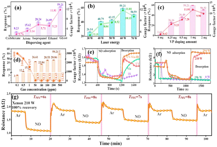
The solvent plays a critical role in the laser ablation of VP, which constraints and collects the splashing VP nanoflakes. The Glycol have the highest response of 59.21% (gauge factor of 1.18 × 10⁵) than those from cyclohexane, acetone, isopropanol, and ethanol (Fig. 4a and Figs. S7a-e in Supporting information). The VP nanoflakes have been detected to have increasing sensing response with increasing laser power from 30 W to 60 W (Fig. 4b and Figs. S7f-j in Supporting information), since higher laser power exfoliate of VP nanoflakes better with more exposed active sites. Some of the VP nanoflake structures are damaged after certain power of laser ablation, resulting in slightly decrease sensing response of VP nanoflakes from laser ablation with power of 60 to 70 W. The optimum amount of VP nanoflakes is 1 mg (Fig. 4c and Figs. S7k-o in Supporting information). The sensing response was detected to increase with increasing amount of VP nanoflakes due to increasing exposure active sites. However, the exposure active sites are not increasing with increasing amount of VP nanoflakes when more than 1 mg since the VP nanoflakes are overlapped with each other. The highest gauge factor was 3.0 × 10⁷ (Fig. 4d and Figs. S7p-x in Supporting information) under 100 ppb, demonstrating to have immense potential in ppb-level sensing.
Figure 4
Figure 4.
(a–d) Sensitivity influence factors. Response of (a) different solvents: cyclohexane, acetone, isopropanol, ethanol, and glycol; (b) different laser power: 30–70 W; (c) different additive amount: 0–2 mg; (d) different concentrations: 50 ppb-500 ppm. (e-g) Recovery of VP/G sensors. The influence of (e) various wavelengths: UV, Vis, IR, UV–vis-IR; (f) different light powers: 0-290 W. (g) Cyclic stability of VP/G sensor under 210 W irradiation.
High gas sensing response with quick and strong adsorption is usually accompanying with difficulty of desorption. Irradiation with different wavelength light was adopted to improve the recovery (Figs. 4e-g). The VP/G were irradiated by different wavelength lights (Fig. 4e). The irradiation of UV and UV-vis-IR lights were effective for the NO desorption, resulting in a fast recovery to its original resistance. The IR light was futile for NO desorption. Meanwhile, the UV-vis-IR is more stable for recovery. The light power was significant for NO desorption (Fig. 4f). The resistance was not recovered when the power is lower than 196 W. The fast recovery was obtained in 210 and 294 W. Considering low-energy, 210 W was chosen for NO desorption. Fig. 4g shows the cyclic stability was measured using irradiation of UV–vis-IR of 210 W for gas desorption. A stable and ultra-fast recovery time of 6–8s was obtained.
The sensing mechanism was investigated by X-ray photoelectron spectroscopy (XPS) and DFT in Fig. 5 and Fig. S8 (Supporting information). A weak peak at 286 eV corresponding to C−N connection was observed after NO gas adsorption (Fig. S8). The P 2p1/2 and 2 p3/2 peaks were detected to shift to higher binding energy after adsorption of NO due to hole doping (Fig. S8d). Two new peaks at 396 and 406 eV corresponding to -NO2 and -P=N−P groups were emerged after NO gas adsorption (Fig. S8e), indicating a bond formation between P and N.
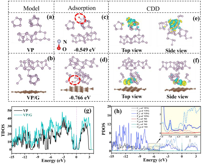
Figure 5
Figure 5.
Adsorption mechanism of VP/G by NO gas in DFT calculation. (a) VP model. (b) VP/G heterojunction model. Most stable adsorbed sites of (c) VP and (d) VP/G. Charge density difference of (e) VP and (f) VP/G. The yellow area represents the accumulation of electrons, and the blue area represents the depletion of electrons, respectively. (g) Total density of states of VP and VP/G. (h) Partial density of states of VP/G after adsorption, and high-resolution of PDOS in the inset.
The VP and VP/G models before adsorption are shown in Figs. 5a and b. The NO molecule was attracted to be close to the five-ring tube without bonding for pure VP (Fig. 5c), where the adsorption energy was −0.549 eV. The adsorption energy of VP/G to NO was −0.766 eV, more stable than that of pure VP. A chemical N−P bond was formed between VP/G and NO close to the graphene sheet as shown in Fig. 5d. The conjugate π electrons of graphene pushed NO molecules to VP and induce the directional arrangement of NO molecules, making N atom more interact with lone pair electrons of P atom. The charge density difference was aroused in a large area by the NO molecule for pure VP (Fig. 5e, yellow area-electron accumulation, blue area-electron depletion). The electrons migrated from P atom of VP/G to N atom of NO molecule to form P−N bond due to the larger electronegativity of N (Fig. 5f). Less than 0.3 e migrated from NO to VP for pure VP, while 0.715 e migrated from VP to NO for VP/G. The more electrons migrated, the stronger the interaction was. It indicates the significant function of graphene for VP sensing. The peaks of VP/G are shifted to the positive direction compared to pure VP from the total density of states (TDOS) of VP and VP/G (Fig. 5g), indicating a stable structure for VP/G for a high NO sensing capability. The partial density of states (PDOS) of P-p, N-p between -7.5 to 5.5 eV were overlapped for VP/G (inset of Fig. 5h), further confirming the bond formation between VP/G and NO (Fig. 5d). All the calculation data are well consistent with the experimental results.
In conclusion, the VP nanoflakes were ablated by laser and tiled on graphene for gas sensing. The VP nanoflakes had 1–5 layers after laser ablation. The ultra-high gauge factor of 3.0 × 10⁷ was detected at room-temperature sensing ppb-level NO. An recovery time was only 6s by irradiation of UV or UV-vis-IR lights. The sensing mechanism was that the electrons were transferred from VP to NO to form a new P−N bond. The adsorption energy of VP/G with NO was calculated to be −0.788 eV, further confirming the electron migration. The calculation data are well consistent with the experimental results.
Declaration of competing interest
The authors declare that they have no known competing financial interests or personal relationships that could have appeared to influence the work reported in this paper.
Acknowledgments
The authors greatly thank the funding support by National Natural Science Foundation of China (Nos. 61705125, 22175136), and Open Foundation of State Key Laboratory of Featured Metal Materials and Life-cycle Safety for Composite Structures, Guangxi University (No. 2022GXYSOF15).
Supplementary materials
Supplementary material associated with this article can be found, in the online version, at doi:10.1016/j.cclet.2023.108199.
S. Hou, R. Pang, S. Chang, et al., ACS Appl. Mater. Interfaces 12 (2020) 29778–29786.
Figure 1
Process flow diagram: (a) Laser ablation of VP, (b) VP/G heterojunction. (c) Sensing performance test. Topography and structure of VP after laser ablation: (d) SEM image, (e) HRTEM image and SAED in the inset, (f) AFM image, (g) Raman spectrum, and (h) XRD spectrum.
Figure 2
Topography and structure of VP/G heterojunction. (a) SEM image with EDS mapping in the inset: (b) P distribution, (c) C distribution, (d) O distribution. (e) Band gap of bulk violet phosphorus, VP and graphene. (f) Raman spectra in 300–500 cm−1. (g) Raman spectra in 100–2800 cm−1. (h) XRD spectra of VP and VP/G.
Figure 3
Gas sensing performance of VP/G. (a) Schematic of VP/G sensor. (b) Selective sensing of VP/G in testing NO and CO. (c) Stability of VP/G based sensor. (d) Gauge factor and (e) Resistance with time for 100 ppb NO sensing. (f) Fitting of gauge factor in sensing 100 ppb NO. (g) Gauge factor and (h) Resistance with time for 500 ppm NO sensing. (i) Fitting of gauge factor of VP/G in sensing 500 ppm NO. (j) Sensitivity comparison with other works [21-37]. (k) Response time, recovery time and working temperature comparison with other works [21-31]. The equilibrium gas is air in ppb-level and inert Ar gas in ppm-level. The amount of VP is 1 mg on 10 × 10 mm2 graphene film. The solvent is glycol.
Figure 4
(a–d) Sensitivity influence factors. Response of (a) different solvents: cyclohexane, acetone, isopropanol, ethanol, and glycol; (b) different laser power: 30–70 W; (c) different additive amount: 0–2 mg; (d) different concentrations: 50 ppb-500 ppm. (e-g) Recovery of VP/G sensors. The influence of (e) various wavelengths: UV, Vis, IR, UV–vis-IR; (f) different light powers: 0-290 W. (g) Cyclic stability of VP/G sensor under 210 W irradiation.
Figure 5
Adsorption mechanism of VP/G by NO gas in DFT calculation. (a) VP model. (b) VP/G heterojunction model. Most stable adsorbed sites of (c) VP and (d) VP/G. Charge density difference of (e) VP and (f) VP/G. The yellow area represents the accumulation of electrons, and the blue area represents the depletion of electrons, respectively. (g) Total density of states of VP and VP/G. (h) Partial density of states of VP/G after adsorption, and high-resolution of PDOS in the inset.

 DownLoad:

 下载:
下载:


