School of Physics and Electronic Science, East China Normal University, Shanghai 200241, China
b.
International Center for Materials Nanoarchitectonics (MANA), National Institute for Materials Science (NIMS), Ibaraki 305-0044, Japan
c.
School of Chemical Engineering and Australian Institute for Bioengineering and Nanotechnology (AIBN), The University of Queensland, Queensland 4072, Australia
d.
Department of Plant and Environmental New Resources, Kyung Hee University, Gyeonggi-do 446-701, South Korea
* Corresponding authors. ** Corresponding author at: International Center for Materials Nanoarchitectonics (MANA)
Received Date:
21 March 2020 Accepted Date:
28 April 2020 Revised Date:
13 April 2020 Available Online:
15 January 2021
Abstract:
Nanoarchitectonics provide versatile opportunities for modifying the properties of coordination polymers (CP) other than molecular engineering. Spatial-controlled etching focuses on the controlled disassembly of the frameworks. The etching method provides an excellent opportunity for tailoring the properties and functions of the CPs. Here, we discuss the mechanism for controlled etching of the CPs and summarized the two main strategies utilized so far. Several examples are illustrated to demonstrate recent developments in this area. Moreover, advantages of the etched CPs are summarized in several important applications, including energy storage, catalysis and nanomedicine.
Crystalline coordination polymers (CPs) or metal-organic frameworks (MOFs) are among the most widely studied of porous materials area in recent years [1-15]. They possess high porosity, large surface area, and highly designable frameworks, leading to their potential applications in a wide range of fields, such as catalysis, energy storage and nanomedicine [1-15]. To meet the practical requirements, the properties of CPs need to be tailored accordingly. Compared to molecular engineering, nanoarchitectonics or nanoengineering may provide a more effective method to tune the porosity of CPs or MOFs. Recently, the controlled etching of CPs has emerged as a sophisticated way to tailor the structure and therefore, the functional performance of CPs [16-20]. Herein, we summarize the latest development on spatial-controlled etching of CPs. First, we illustrate some remarkable examples based on different etching mechanisms, i.e., direct-etching and surface-protected etching process. Second, we show applications of these etched CPs in sodium-ion batteries (SIBs), supercapacitors, catalysis, nanomedicine, etc.
2.
Etching strategies
Various etching strategies have been developed to realize versatile CPs nanoarchitectures have been developed, including direct etching which is induced by structural inhomogeneity, and surface-protected etching assisted by functionalization agents. A brief introduction of the two etching strategies is summarized below.
2.1
Direct etching
CPs are built up from metal ions/clusters and molecular ligands. Intrinsically, some coordination sites are less stable than others. Furthermore, many defects such as vacancies, dislocations or grain boundaries exist in the crystal. These defects decrease chemical stabilities at the surrounding locations. The inhomogeneous distribution of unstable sites in a crystal makes spatial-controlled etching to be possible [21]. When a crystal is immersed in acidic or alkaline solutions, a direct etching becomes possible. Representative etching agents includes hydrochloric acid (HCl), acetic acid, ammonia and so on.
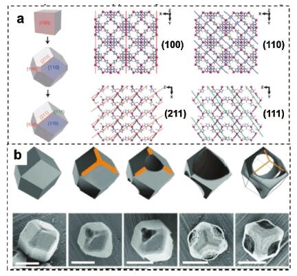
By exploiting the weak stability of the metal-ligand coordination bonds, Avci and co-workers employed a solution-based anisotropic etching of colloidal zeolitic-imidazolate framework (ZIF) crystals to fabricate ZIF-8 microcages [22]. Anisotropic etching is usually used in microelectronics manufacturing to fabricate nanostructures on silicon wafers. For ZIF-8 crystals, the exposed crystallographic planes vary depending on the morphology with distinct atomic packing on different planes. For example, there are several Zn-2-methylimidazole coordination bonds on the (100) and (211) planes, while the (111) and (110) planes do not have such bonds, as shown in Fig. 1a. Based on aforementioned differences, when rhombic dodecahedral ZIF-8 crystals were immersed in a xylenol orange (XO)/HCl etchant solution at room temperature, a much higher etching rate of the (100) and (211) planes is observed. During this etching process, XO not only provided protons, but also worked as a chelating agent to coordinate with ZnII ions. After etching, the crystal structure of the residual ZIF-8 crystals remained unchanged. However, the edges of the crystal were maintained, resulting in a cage-like structure (Fig. 1b). Colloidal ZIF-8 hexapods have been prepared by the etching of convex polyhedron ZIF-8 particles, as demonstrated by Ou et al. [23]. In order to elucidate how the parent ZIF-8 crystals were converted into hexapod morphology, they monitored the progress of the in situ etching process via direct visualization with optical microscope. This real-time optical imaging method provided the opportunity to understand the etching mechanism of CPs.
Figure 1
Figure 1.
(a) Schematic diagram of the crystal structure of the exposed crystallographic planes of ZIF crystals. (b) Schematic illustration of the change in crystal morphology during the etching of rhombic dodecahedral ZIF-8 crystals. Scale bars: 1 μm. Copied with permission [22]. Copyright 2015, Wiley-VCH.
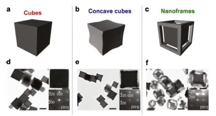
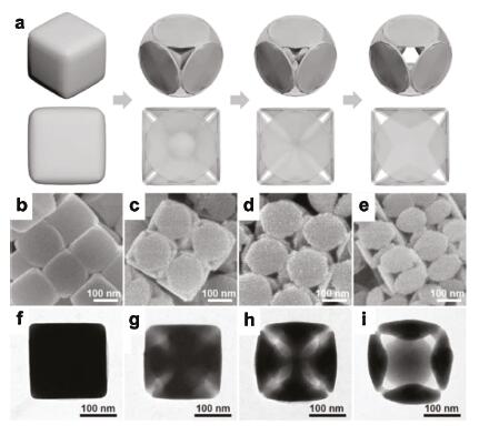
Protons and hydroxide ions show different preferences in the etching of CPs crystals. In the cases of Prussian Blue analogues (PBAs), H+ ions prefer the faces, while OH– ions prefer the corners. For instance, when Ni-Fe PBA cubes were etched by HCl (0.5 mol/L), the H+ ions preferentially attacked the central area of the faces of a cubic crystal, leading to a faster dissociation of the faces than the edges [24]. As a result, the initial Ni-Fe PBA cubes were converted into Ni-Fe PBA concave nanocubes at first, before becoming monocrystalline nanoframes. The morphological evolution is illustrated in Fig. 2. When ammonia is used as the etchant, it provides OH– ions [25]. Nai et al. reported the etching of Ni-Fe PBA cubes by using ammonia (28%–30%) at room temperature [26]. Nanocages with open frameworks and hollow interiors were obtained after etching. By means of Fourier transform infrared (FT-IR) spectra and time-dependent transmission electron microscopy (TEM) analysis, the NiII-N≡C-FeIII and NiIII-N≡C-FeII species are found to coexist within the Ni-Fe PBA crystals. The NiII-N≡C-FeIII species are located mainly at the center, while the NiII-N≡C-FeII is located near the surface of the crystals. Time-dependent observations indicated that the etching occurred preferentially with the NiII-N≡C-FeIII species rather than NiII-N≡C-FeII due to the stronger affinity of the FeIII species to the -CN- group (Fig. 3). Based on the same etchant, Han et al. fabricated Ni-Co PBA nanocages which were constructed of pyramidal walls [27]. The key point is that there were richer number of defects in the center of the Ni-Co PBA crystals than in the external parts, because dissolution-recrystallization can reduce defects in the external part of the crystals. The parts with more defects could be removed faster than the other parts, resulting in preferential hollowing of the interior cores. The relevant TEM image shows the unique pyramid-like walls of the obtained nanocages. Furthermore, Feng et al. converted Co-Co PBAs microcubes into microframes by using ammonia (28%–30%) as the etchant [28]. This anisotropic etching process was ascribed to the different reactivity of corner and plane surfaces of PBA microcubes because of complexation between NH3 and Co2+ from Co-Co PBAs. The average thickness of the obtained microframes was 80 nm.
Figure 2
Figure 2.
(a-c) Schematic illustration of the formation of Ni-Fe PBA nanoframes. (d) Ni-Fe PBA cubes. (e) Ni-Fe PBA concave cubes. (f) Ni-Fe PBA nanoframes. Scale bars: left (100 nm), middle (200 nm), right (100 nm), and inset images (50 nm). Copied with permission [24]. Copyright 2016, Wiley-VCH.
Figure 3.
(a) Schematic illustration of the fabrication process of Ni-Fe PBA nanocages. (b–e) FESEM and (f–i) TEM images of Ni-Fe PBA nanocages obtained after etching for (b, f) 0 min, (c, g) 1 min, (d, h) 3 min and (e, i) 5 min in ammonia at room temperature. Copied with permission [26]. Copyright 2017, Wiley-VCH.
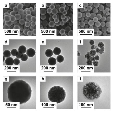
Temperature can serve as a measure to control the etching of CPs. Recently, Ren and co-workers investigated the role of etching temperatures on the synthesis of hierarchically porous Fe[Fe(CN)6] nanospheres. Fig. 4 illustrates that roughness of the surface of the particles varied with different etching temperature. Compared with pristine Fe[Fe(CN)6] nanospheres, the surface area was enlarged from 88 m2/g to 368 m2/g after etching at 100 ℃ [29].
Figure 4
Figure 4.
Fabrication of hierarchical porous hollow Fe[Fe(CN)6] nanospheres at different temperatures. SEM and TEM images at (a, d, g) 80 ℃, (b, e, h) 100 ℃ and (c, f, i) 120 ℃, respectively. Copied with permission [29]. Copyright 2019, the Royal Society of Chemistry.
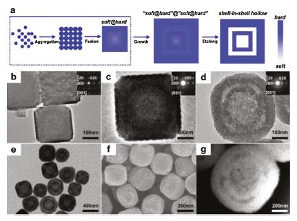
The etching process cannot only be used to construct hollow structure, but can also be used to prepare more sophisticated structures, such as multishelled crystals [30]. Hu et al. established a step-by-step growth and etching strategy to fabricate PBAs with multishelled nanoarchitectures [31]. The strategy involved the epitaxial deposition of multilayers, and subsequent removal of the interfaces among the layers. Preferential removal of the interfaces occurred because of the large number of defects among the layers. After epitaxial deposition, less defects were observed in the shell, and a core-shell structure was formed (Fig. 5a). The core contained more defects and was referred to as the "soft" part, while the shell with less defects was denoted as the "hard" part. Further deposition of additional PBA layers on these "soft@hard" particles led to a "soft@hard@soft@hard" structures. When these particles were dispersed in a hot HCl solution, the interfaces with more defects were removed at a faster rate. Therefore, the "soft" core was removed, while the "hard" shell was preserved, leading to the 'shell-in-shell' structure. As shown in Figs. 5b-g, the final product was single crystalline and it could be used as a seed to fabricate a double yolk-shell structure.
Figure 5
Figure 5.
(a) Schematic illustration of the step-by-step processes to fabricate PB with multilayer nanoarchitectures. (b) TEM image of the PB seeds. (c) TEM image of "soft@hard"@"soft@hard" particle. (d) TEM image of shell-in-shell particle after chemical etching. (e) Low-magnification TEM image of shell-in-shell particles. (f) SEM image of shell-in-shell particles. (g) HAADF-STEM image of a shell-in-shell particle. Copied with permission [31]. Copyright 2013, American Chemical Society.
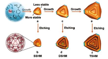
The step-by-step crystal growth and etching strategy was used by Liu and co-workers to prepare multishelled hollow chromium(III) terephthalate CPs (MIL-101) [32]. Specifically, inhomogeneous MIL-101 crystals with octahedral shape were prepared by layer-by-layer growth, followed by etching with acetic acid at 180 ℃ for 4 h (Fig. 6). Heterogeneity of the crystal was partly due to the nucleation process. In order to minimize the surface energy, a small unit of coordination polymer rapidly nucleated to form the core part. During the subsequent stage, nucleation became difficult as the concentration of the reactants was decreased. Instead, the slow growth of the outer layer led to less defects in the outer layer than in the inner core. When the multilayered MIL-101 crystals with unevenly distributed defects were placed into a hot acetic acid solution, H+ ions diffused into the core through the channels, preferentially etching the defective regions. Finally, a multilayered hollow structure was obtained.
Figure 6
Figure 6.
Fabrication of single-, double- and triple-shelled hollow MIL-101, which are denoted as SSHM, DSHM and TSHM, respectively. Copied with permission [32]. Copyright 2017, Wiley-VCH.
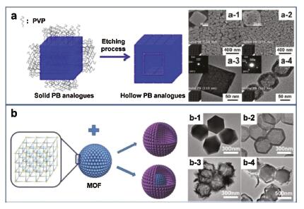
In addition to direct etching, another etching approach for CPs is surface-protected etching which involves the use of protective agent to control etching sites. Polymers are particularly useful for surface protection. Hu et al. reported the synthesis of hollow PB particles in the presence of polyvinylpyrrolidone (PVP) (Fig. 7a) [33-35]. In brief, PB mesocrystals were initially formed by the aggregation of nanocrystals. Before etching, PVP was coated on the surface of PB mesocrystals by coordination between the amide group of PVP and the iron ions of PB crystals. After that, the PB particles were treated with HCl solution at 140 ℃ for 4 h. Protons diffused into the core of the mesocrystals, removing the inner core of particles. After etching, crystals with hollow interiors were obtained. The selected area electron diffraction (SAED) pattern indicated that the single-crystalline nature of these hollow particles was still retained. There were two crucial points for successful etching: 1) PB mesocrystals were used. When PB single crystals were etched under the same conditions, the interior cavity had to be created due to the obstacles for the protons to travel inside. 2) The surface of the PB crystals should only be partially protected. Neither fully protected nor non-protected particles could be selectively etched. Apart from PVP, cetyltrimethylammonium bromide (CTAB) could also serve as a protective agent during the selective etching [36]. Impressively, this strategy was applicable to other PBAs, such as Co-Fe PBA, Ni-Fe PBA.
Figure 7
Figure 7.
(a) Schematic illustration of the formation of hollow PB nanocubes by using PVP as a protective agent. Corresponding SEM images (a-1,2) and TEM (a-3,4) images of PB mesocrystals. (b) Schematic representation of the formation process of hollow ZIF-8 with the use of TA/GA as a protective agent. TEM images of ZIFs before and after etching. Copied with permission [33-35, 40]. Copyright 2012, American Chemical Society. Copyright 2012, Wiley-VCH. Copyright 2012, American Chemical Society. Copyright 2016, Wiley-VCH.
In addition to the use of additional protective ageants, some agents can simultaneously act as both protective and etching agents. Phenolic acids, including tannic acid (TA) and gallic acid (GA) have been shown to function as both etching and surface functionalization agents [37-39]. For example, hollow ZIF-8 crystals were formed with the assistance of TA (Fig. 7b) [40]. TA is a natural polyphenol which is composed of multiple phenolic units, allowing it to coordinate with metal ions to form metal-phenolic networks. Once metal-phenolic networks are formed, the surface of the ZIF-8 crystals is changed from hydrophobic to hydrophilic. As a result, protons preferred to diffuse through the functionalized pores into the inner cavities of the crystals. The protons destroyed the inner cores of the crystals, producing hollow ZIF-8 crystals with intrinsic crystalline frameworks. Interestingly, when the more acidic GA is used as an etchant, the shells of the prepared hollow ZIF-8 polyhedrons became composed of several nanosheets, mainly derived from the uneven protection of GA on the surface of the ZIF-8 particles. Similarly, MIL-68 (In) microrods have been prepared by etching with TA. Superior to the self-assembly or layer-by-layer tailoring of CPs, this method provides a facile strategy to localize a void precisely inside the CPs.
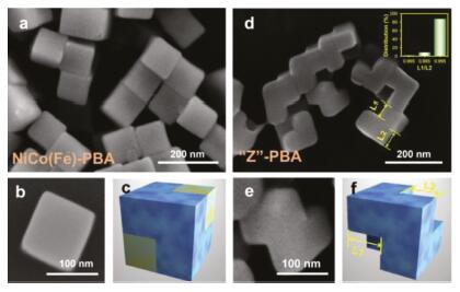
Besides using protective agent, the crystal structure can be programed in order to direct the subsequent etching sites. Tu et al. intentionally designed reactive sites into a MOF single crystal. After immersing the crystal into corrosive solution, the reactive sites were removed, leaving ordered vacancies inside [41]. Ye et al. pre-doped metals and ligands (i.e., [Fe(CN)6]3−) into NiCo PBA cubes. Subsequently, anisotropic etching happened [42]. Fig. 8 showed that peculiar zigzag-like crystals were acquired. In order to unveil the underlying mechanism, metal-doped and metal-ligand codoped parent PBAs were investigated, respectively. When Fe3+ was as doped into the NiCo PBA, the particles were dissolved completely after etching. Alternatively, the NiCo(Fe) PBA prepared by codoping of [Fe(CN)6]3- showed an asymmetrical etching characteristic. Only two out of eight corners of cubes were etched. Survey XPS data indicated that the pristine NiCo(Fe) PBA exhibited both FeII and FeIII, but only single FeII existed after etching. Hence, the formation of "Z"-PBA PBA was attributed to the release of FeIII.
Figure 8
Figure 8.
(a) Low- and (b) high-magnification SEM images, and (c) the corresponding schematic illustration of NiCo(Fe)-PBA. (d) Low and (e) high-magnification SEM images, and (f) the corresponding schematic illustration of "Z"-PBA. Copied with permission [42]. Copyright 2019, the Elsevier B.V.
Etching provides alternated performance in various applications such as energy storage, catalysis and nanomedicines.
3.1
Sodium-ion batteries (SIBs) and supercapacitors (SCs)
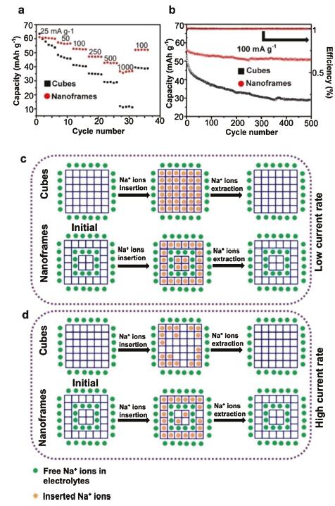
Based on the wide availability and low cost of sodium, SIBs are considered as a potential alternative to lithium-ion batteries, with potential applications in large-scale energy storage or next-generation energy storage devices [43-45]. For the sake of higher power density and energy density, tremendous efforts have been made toward the design and fabrication of electrode materials with novel structures [45-48]. PBAs have been regarded as promising electrode materials for SIBs as they can effectively transport sodium ions [49, 50]. In order to enhance the cycling stability and rate performance of SIBs, frame-structured Ni-Fe PBAs were prepared by controlled etching (Fig. 9) [24]. The frame-like structure effectively increased the contact area between the electrode and electrolyte and shortened the diffusion distance for sodium ions. The resulting Ni-Fe PBA nanoframes exhibited superior rate performance than their cubic counterpart. At a current density of 1 A/g, the capacity retention ratio of the nanoframe-based electrode was as high as 61%, while the cube-based electrode was only 17%.
Figure 9
Figure 9.
(a) Rate capabilities of Ni-Fe PBA cubes and nanoframes as cathode for SIBs. (b) Cycling performance of Ni-Fe PBA cubes and nanoframes as cathode for SIBs. (c) Schematic diagram of Na-ion insertion/extraction of Ni-Fe PBA cubes and nanoframes at low current rates. (d) Schematic diagram of the Na-ion insertion/extraction process in Ni-Fe PBA cubes and nanoframes at high current rates. Copied with permission [24]. Copyright 2016, Wiley-VCH.
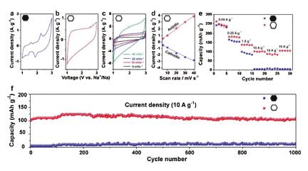
In addition to using the etched CPs directly for SIBs, derivatives of the etched CPs were widely studied for SIBs [51-53]. For instance, hollow carbon nanobubbles were previously obtained by direct carbonization of ZIF-8 nanobubbles [54]. As shown in Fig. 10, non-hollow carbon nanoparticles exhibited obvious redox peaks in the range of 1.5–3.0 V and 0.0–0.5 V, while the CV curve of the hollow carbon nanobubbles showed a rectangular shape with no recognizable redox peak. The change in the CV curves suggested that storage of sodium ions in the hollow carbon nanobubbles became pseudocapacitor-type ion storage. The solid carbon nanobubbles experienced a sharp decline in electrochemical performance. The hollow carbon nanobubbles maintained a respectable capacity of 80 mAh/g at a high current density of 15 A/g. In contrast, the non-hollow carbon nanobubbles experienced a much sharper decline in capacity at 15 A/g. For the hollow carbon nanobubbles, the electrochemical reaction occurred only at the shell, leading to a fast ion storage rate. Therefore, at a high current density of 10 A/g, there was almost no significant loss in the reversible capacity even after 1000 cycles.
Figure 10
Figure 10.
CV curves of the non-hollow carbon (a) and hollow carbon nanobubbles (b) between 1 V and 3 V (vs. Na+/Na) at a potential sweep rate of 5 mV/s. (c) CV curves of the hollow carbon nanobubbles between 1 V and 3 V (vs. Na+/Na) at various rates from 5 mV/s to 40 mV/s. (d) Dependence of anodic and cathodic currents (at 2 V) on scan rate. (e) Rate performances of non-hollow and hollow carbon nanobubbles. (f) Cycling performances of non-hollow and hollow carbon nanobubbles. Copied with permission [54]. Copyright 2017, the Royal Society of Chemistry.
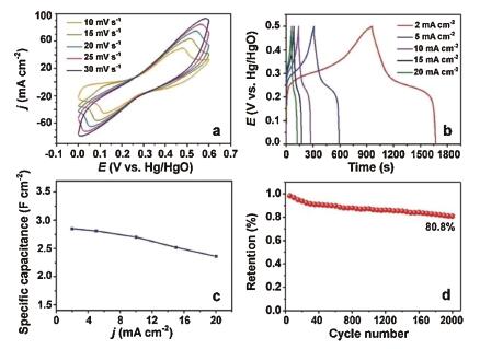
Supercapacitors are considered to be one of the most promising energy storage devices due to their high power density, long-term stability, fast charge/discharge speed and excellent safety [55, 56]. Due to their tunable porosity, high surface area, and excellent capability for insertion of guest ions, CPs exhibit huge potential for advanced SCs [57-59]. However, it is generally believed that the low conductivity and poor stability limit their application as electrode materials [60, 61]. Instead, porous materials derived from CPs have shown enhanced electrochemical performance [57, 62-64]. For instance, Song et al. adopted an ion exchange/etching strategy for constructing CP-derived hollow (Ni, Co)Se2-carbon cloth electrode [65]. Owing to the hollow structure and bimetallic composition, the performance of the as-obtained electrode for supercapacitors was remarkable. As shown in Fig. 11, the specific capacitance was as high as 2.85 F/cm2 at a small current density with a favorable cycling stability (80.8% retention of the capacitance) after 2000 cycles. Ion-exchange/etching strategy was developed by Le and co-workers to fabricate hierarchical core-shell hollow Fe-Co-S nanoarrays on Ni foam by using 2D Co-MOF as sacrificial templates [66]. Taking advantage of the unique structural merits, the Fe-Co-S nanoarrays displayed an outstanding cycling stability with a capacitance retention of 89.6% after 5000 cycles at 5 A/g when tested as electrode in an alkaline electrolyte. Jiang and co-workers utilized precipitation and simultaneous acidic etching of ZIF-67 to obtain Co-based layered double hydroxide (LDH) nanocages [67]. Among them, Ni-Co LDH nanocages showed superior pseudocapacitance and long-term electrochemical stability. The hierarchical structure assembled by ultrathin nanosheets helped to maintain the morphology and prevented aggregation and deactivation during the redox reactions.
Figure 11
Figure 11.
Electrochemical performance of the (Ni, Co)Se-carbon cloth electrode. (a) CV curves. (b) Galvanostatic charge–discharge curves at different current densities. (c) Specific capacitance. (d) Cycling performance. All measurements were performed in 6 mol/L KOH solution. Copied with permission [65]. Copyright 2019, the Royal Society of Chemistry.
The rapid consumption of fossil fuels and related environmental problems have raised interests in the research and development of renewable energy systems. Electrochemical water splitting produces hydrogen and oxygen in an environmentally-friend way [68]. However, the slow kinetics of the anodic oxygen evolution reaction (OER) have limited the wider utilization of water splitting technology [69-71]. Therefore, catalysts are needed to promote OER at a low overpotential (η) to improve the energy conversion efficiency. Open structure is introduced to increase the contact area between electrode and electrolyte, and provide more reactive sites to improve the catalytic activity [72-74]. By using etched Ni-Co PBAs as precursors, Ni-Co oxide nanocages were obtained after the thermal treatment in air [27]. Compared to nanocubes, the nanocages had a larger electrochemically active surface area, leading to moreactive sites. This led to both improved OER activity and stability (Fig. 12). Zhang and co-workers utilized NaOH as an etching agent to prepare macroporous bimetallic MOF crystals [75]. The obtained crystals exhibited superior activities for hydrogen evolution reaction (HER) and OER in an alkaline electrolyte. To deliver a current density of 10 mA/cm2 for HER, the macroporous MOF crystals only needed an overpotential of 43 mV, which is comparable to commercial noble metal catalysts. Furthermore, the macroporous MOF crystals showed a lower overpotential of 198 mV for OER compared to commercial RuO2 (250 mV).
Figure 12
Figure 12.
(a) Polarization curves, (b) Tafel plots and (c) chronoamperometry curves of the NiCo mixed oxide cages and porous cubes. Copied with permission [27]. Copyright 2016, Wiley-VCH.
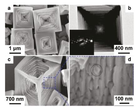
Early studies on noble metal catalysts reveal that hollow and hierarchically porous structures are beneficial for enhancing their catalytic activity [76, 77]. The hollow structure generally has a high surface-to-volume ratio, which enlarges the exposed surface of the catalyst and provides more active sites [78, 79]. In order to optimize the functional performance of CPs in catalysis, selective etching was employed [23, 80]. Bu et al. synthesized CPs with hierarchical structures by combining self-aggregation and etching method (Fig. 13) [81]. In a typical process, hollow Prussian white (PW) crystals were formed by direct etching of the mesocrystals. Owing to the formation of defects, preferential etching resulted in the step-like detachment of nanoparticles. The hierarchical structure enlarged specific surface area of the PW crystals and increased the catalytic activity for Fenton reaction. Ye and co-workers prepared a 3D zigzag-structured PBA by preferential etching [42]. The zigzag-structured PBA exhibited good catalytic activity for the degradation of bisphenol A. With a small dose of the zigzag PBA catalyst (0.1 mg/L), 30 ppm of bisphenol A could be removed, while the cubic PBA could not.
Figure 13
Figure 13.
Electron microscopy images of hierarchical PW crystals. (a) Overview of the crystals. (b) TEM image and SAED pattern (inset) of an individual particle. (c, d) High-magnification SEM images taken from specific sites. Copied with permission [81]. Copyright 2014, the Royal Society of Chemistry.
Overall, the catalytic activity of the CP crystals can be significantly enhanced by etching, because etching can enlarge the accessible surface area, increase the number of catalytically active sites and facilitatemass transport.
3.3
Nanomedicine
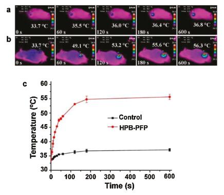
With the development of drug delivery and cancer treatment, CPs are considered to be excellent candidates for nanomedicine due to their excellent biodegradability, low cytotoxicity and multifunctionality [82, 83]. The drug loading and release capacities are controlled by several important factors, including surface area, pore size, and guest-host interactions. To achieve both large loading and controlled release of drugs, CPs with hollow structures and open pores are highly desired [84]. Gao and colleagues previously reported hollow Fe-MOF-5-NH2 crystals via a facile solvothermal method [85]. The drug loading amount was increased by 35% as a result of the hollow morphology. Moreover, the hollow Fe-MOF-5-NH2 crystals could be used for targeted drug delivery, pH-controlled drug release, and magnetic resonance/fluorescence imaging by grafting biomolecules. Jia and co-workers prepared a novel photothermal conversion agent by using hollow mesoporous Prussian blue (HPB). The n-perfluoropentane-encapsulated HPB with excellent colloidal stability played a role for in vivo tumor diagnosis and regression [86]. Since HPB could absorb near-infrared irradiation and effectively convert photon energy into heat, thermal therapy for tumor became possible [87]. The photothermal (PPT) effect of the HPB was investigated in Helaxenograft bearing Balb/c nude mice. As shown in Fig. 14, the tissue containing HPB showed a higher temperature rise under irradiation. The tumor injected with the n-perfluoropentane-encapsulated HPB, was rapidly heated from 33.7 ℃ to 56.3 ℃ within 600 s. The in-vivo photothermal experiments showed that the volume of the tumor was reduced significantly after 7 days, and the tumor recurrence was not found after 28 days.
Figure 14
Figure 14.
(a) Control and (b) treatment group under irradiation. (c) Temperature-change curves of the tumors in each group after irradiation. Copied with permission [86]. Copyright 2015, American Chemical Society.
In conclusion, the controlled etching of CPs has been developed together with the increased understanding of heterogeneity of the CPs crystals. By exploiting intrinsic defects or inducing defects, the spatial-controlled etching of CPs has been realized. The key point is the local instability of the CPs crystals against etchants. Direct and surface-protection assisted etching are two main strategies which have been used to achieve the controlled etching of CPs crystals. These strategies bring about several structural advantages, such as exposed active sites, kinked surfaces, meso/macro-sized pores, connected channels, and high specific surface areas, to the CPs crystals. These features are useful for enlarging the contact surface area between electrode and electrolyte, introducing more active sites, providing effective diffusion channels for mass or ion transport. Applications which strongly rely on these properties are benefited from the controlled etching of CPs. Other applications such as electronic, magnetic or optical sensing may also benifited from the etching of CPs crystals. For instance, the piezoelectric properties of the CP crystals may be controlled by changing the symmetry of crystals after etching. The properties tunability of CPs can enable the tailoring of the sensitivity or selectivity of devices made with CP crystals.
In the future, the controlled etching of CPs may be applied in the development of CP thin films and devices. We should be able to work with thin films and the related devices to precisely introduce patterns, point defects, and other features to meet the requirements for specific applications. Methods other than wet etching should be developed. For instance, laser, plasma, vapor, and other dry etching strategies should be developed. In particular, 3D printing techniques may be integrated with the etching methods to construct complex structures in a rapid and efficient manner.
Declaration of competing interest
The authors declare that they have no known competing financial interests or personal relationships that could have appeared to influence the work reported in this paper.
Acknowledgments
This work was supported by National Natural Science Foundation of China (No. 21473059). This work was partly performed at the Queensland node of the Australian National Fabrication Facility (ANFF), a company established under the National Collaborative Research Infrastructure Strategy to provide nano and micro-fabrication facilities for Australian researchers.
* Corresponding authors. ** Corresponding author at: International Center for Materials Nanoarchitectonics (MANA), National Institute for Materials Science (NIMS), Ibaraki 305-0044, Japan. E-mail addresses: KANETI.Valentino@nims.go.jp (Y.V. Kaneti), mhu@phy.ecnu.edu.cn (M. Hu), y.yamauchi@uq.edu.au (Y. Yamauchi).
[1]
S. Kitagawa, R. Kitaura, S.I. Noro, Angew. Chem. Int. Ed. 43 (2004) 2334-2375. doi: 10.1002/anie.200300610
[2]
O.M. Yaghi, M. O'Keeffe, N.W. Ockwig, et al., Nature 423 (2003) 705-714. doi: 10.1038/nature01650
[3]
A. Azhar, Y. Li, Z. Cai, et al., Bull. Chem. Soc. Jpn. 92 (2019) 875-904. doi: 10.1246/bcsj.20180368
[4]
Y.Z. Chen, R. Zhang, L. Jiao, H.L. Jiang, Coord. Chem. Rev. 362 (2018) 1-23. doi: 10.1016/j.ccr.2018.02.008
[5]
J.M. Lin, C.T. He, Y. Liu, et al., Angew. Chem. Int. Ed. 55 (2016) 4674-4678. doi: 10.1002/anie.201511006
Figure 1
(a) Schematic diagram of the crystal structure of the exposed crystallographic planes of ZIF crystals. (b) Schematic illustration of the change in crystal morphology during the etching of rhombic dodecahedral ZIF-8 crystals. Scale bars: 1 μm. Copied with permission [22]. Copyright 2015, Wiley-VCH.
Figure 3
(a) Schematic illustration of the fabrication process of Ni-Fe PBA nanocages. (b–e) FESEM and (f–i) TEM images of Ni-Fe PBA nanocages obtained after etching for (b, f) 0 min, (c, g) 1 min, (d, h) 3 min and (e, i) 5 min in ammonia at room temperature. Copied with permission [26]. Copyright 2017, Wiley-VCH.
Figure 4
Fabrication of hierarchical porous hollow Fe[Fe(CN)6] nanospheres at different temperatures. SEM and TEM images at (a, d, g) 80 ℃, (b, e, h) 100 ℃ and (c, f, i) 120 ℃, respectively. Copied with permission [29]. Copyright 2019, the Royal Society of Chemistry.
Figure 5
(a) Schematic illustration of the step-by-step processes to fabricate PB with multilayer nanoarchitectures. (b) TEM image of the PB seeds. (c) TEM image of "soft@hard"@"soft@hard" particle. (d) TEM image of shell-in-shell particle after chemical etching. (e) Low-magnification TEM image of shell-in-shell particles. (f) SEM image of shell-in-shell particles. (g) HAADF-STEM image of a shell-in-shell particle. Copied with permission [31]. Copyright 2013, American Chemical Society.
Figure 6
Fabrication of single-, double- and triple-shelled hollow MIL-101, which are denoted as SSHM, DSHM and TSHM, respectively. Copied with permission [32]. Copyright 2017, Wiley-VCH.
Figure 7
(a) Schematic illustration of the formation of hollow PB nanocubes by using PVP as a protective agent. Corresponding SEM images (a-1,2) and TEM (a-3,4) images of PB mesocrystals. (b) Schematic representation of the formation process of hollow ZIF-8 with the use of TA/GA as a protective agent. TEM images of ZIFs before and after etching. Copied with permission [33-35, 40]. Copyright 2012, American Chemical Society. Copyright 2012, Wiley-VCH. Copyright 2012, American Chemical Society. Copyright 2016, Wiley-VCH.
Figure 8
(a) Low- and (b) high-magnification SEM images, and (c) the corresponding schematic illustration of NiCo(Fe)-PBA. (d) Low and (e) high-magnification SEM images, and (f) the corresponding schematic illustration of "Z"-PBA. Copied with permission [42]. Copyright 2019, the Elsevier B.V.
Figure 9
(a) Rate capabilities of Ni-Fe PBA cubes and nanoframes as cathode for SIBs. (b) Cycling performance of Ni-Fe PBA cubes and nanoframes as cathode for SIBs. (c) Schematic diagram of Na-ion insertion/extraction of Ni-Fe PBA cubes and nanoframes at low current rates. (d) Schematic diagram of the Na-ion insertion/extraction process in Ni-Fe PBA cubes and nanoframes at high current rates. Copied with permission [24]. Copyright 2016, Wiley-VCH.
Figure 10
CV curves of the non-hollow carbon (a) and hollow carbon nanobubbles (b) between 1 V and 3 V (vs. Na+/Na) at a potential sweep rate of 5 mV/s. (c) CV curves of the hollow carbon nanobubbles between 1 V and 3 V (vs. Na+/Na) at various rates from 5 mV/s to 40 mV/s. (d) Dependence of anodic and cathodic currents (at 2 V) on scan rate. (e) Rate performances of non-hollow and hollow carbon nanobubbles. (f) Cycling performances of non-hollow and hollow carbon nanobubbles. Copied with permission [54]. Copyright 2017, the Royal Society of Chemistry.
Figure 11
Electrochemical performance of the (Ni, Co)Se-carbon cloth electrode. (a) CV curves. (b) Galvanostatic charge–discharge curves at different current densities. (c) Specific capacitance. (d) Cycling performance. All measurements were performed in 6 mol/L KOH solution. Copied with permission [65]. Copyright 2019, the Royal Society of Chemistry.
Figure 13
Electron microscopy images of hierarchical PW crystals. (a) Overview of the crystals. (b) TEM image and SAED pattern (inset) of an individual particle. (c, d) High-magnification SEM images taken from specific sites. Copied with permission [81]. Copyright 2014, the Royal Society of Chemistry.
Figure 14
(a) Control and (b) treatment group under irradiation. (c) Temperature-change curves of the tumors in each group after irradiation. Copied with permission [86]. Copyright 2015, American Chemical Society.

 DownLoad:


 下载:
下载:


