Citation:
Fan Haochen, Huang Jinhua, Jiang Kejian, Song Yanlin, Zhou Xueqin. All Solution-Processed Planar Heterojunction Organic Solar Cells Using A Highly Crystalline Squaraine Dye[J]. Chemistry,
2020, 83(11): 1007-1013.
Received Date:
26 June 2020 Accepted Date:
22 July 2020 Available Online:
01 November 2020
Abstract:
Highly crystalline organic semiconductors with close molecular stacking could hold high charge mobility but low solubility in common organic solvents, limiting their solution processability for organic optoelectronics. Herein, a methyl-decorated high-crystalline squaraine dye (DM-SQ) is synthesized, and a highly crystalline thin film is solution-deposited using trifluoroacetic acid (TFA) as solvent. The resultant film shows a higher hole mobility as compared with that of the vacuum-deposited film (5.28×10⁻⁴ vs. 7.53×10⁻⁵ cm2·V-1·s-1). With DM-SQ as donor and PC61BM (phenyl-C61-butyric acid methyl ester) as acceptor, the solution-processed planar heterojunction solar cells exhibit an average power conversion efficiency of 6.08±0.19%, higher than 3.56±0.22% for the vacuum-deposited devices.
Organic solar cells (OSCs) have attracted increasing attention due to their potential low cost, lightweight, flexibility, and large-area fabrication[1]. OSCs can be fabricated via the easy solution-processing and/or vacuum-deposition appr-oach. The solution-processed OSCs are normally fabricated using halogenated or non-halogenated organic solvents such as 1, 2-dicholorobenzene and xylene. Decoration of organic semiconductors with long alkyl chains and/or bulky groups is usually employed to ensure their solution processability. With vigorous efforts in materials, device archite-ctures and interface engineering, the power conver-sion efficiency (PCEs) of the solution-processing OSC has been raised up to 17%[2].
Planar heterojunction cells would offer simpler large-scale production and better long-term stability, where a light absorber with high charge mobility with exciton diffusion length is required for high-efficiency devices. Organic dyes such as squaraine (SQ) have unique photophysical and photochemical properties such as high absorption coefficients (on the order of 105 cm-1) with tunable bandgaps in the visible and near-infrared regions, as well as high photochemical and thermal stability[3]. They have received increasing attention in xerographic photoreceptors[4], optical recording[5], nonlinear optics[6], and solar cells[7]. However, they are normally insoluble in commonly used solvents such as 1, 2-dichlorobenzene (o-DCB), chlorobenzene (CB), and xylene. With decoration of long alkyl chains and/or bulky groups, a series of soluble SQ dyes, 2, 4-bis[4-(N, N-diaryl or alkylamino)-2, 6-dihydroxyphenyl] squaraine, have been developed for solution-processed OSCs, and the PCEs of 4%~6% have been obtained[8]. Such decoration, on the other hand, would disturb the intermolecular charge transfer interaction between the adjacent molecules due to the steric effect, thus deteriorating their charge mobilities and exciton diffusion lengths, which would in turn deteriorate device performance[9]. Studies have pointed out that shortening the alkyl chain length can effectively improve the photoconductivity and charge mobility[10].
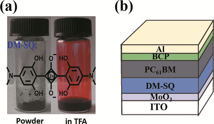
In this paper, a new squaraine dye (DM-SQ, Fig. 1a), 2, 4-bis[4-(N, N-dimethylamino)-2, 6-dihydroxyphenyl] squaraine, was prepared. In the dye molecule, short methyl chains were introduced, resulting in high crystalline but much low solubility as compared to the commercial N-isopropyl SQ dye[8n]. As a result, the DM-SQ dye could not be processed using common organic solvents such as o-DCB, CB and xylene. However, we found that the electron-rich DM-SQ dye could be dissolved in trifluoroacetic acid (TFA) with good solution processability, and the solution-processed film holds high crystalline with high hole mobility up to 5.28×10⁻⁴ cm2 ·V-1 ·s-1. Accordingly, double-layered OSCs are feasibly fabricated via the solution-processed method with PCEs of 6.08±0.19%.
DM-SQ was synthesized via a condensation reaction between 5-N, N-dimethylamino-1, 3-dihy-droxybenzene and squaraine acid as described in the literature with a yield of 94.4%[11, 12]. The raw product was purified via acid pasting (by TFA), Soxhlet extraction and further vacuum sublimation. 1H NMR (101 MHz, CF3COOD) δ: 7.53(s, 2H),4.43 (s, 12H); 13C NMR (101 MHz, solid): 40.52, 94.70, 102.28, 158.87, 162.79, 181.01; MS (HR-MALDI-TOF), m/z: calcd. For (C20H21N2O6): 385.139682,Found: 385.139413.
1.2
Device fabrication
OSCs with a typical configuration of ITO/MoO3/DM-SQ/PC61BM/Buthocuproine(BCP)/Al. All devices were fabricated on commercial indium-tin oxide (ITO) coated glass. Before use, the glass was pre-cleaned with deionized water, CMOS grade acetone and isopropanol in turn for 15 min. The organic residues were further removed by treating with UV-ozone for 1 h. The MoO3 films (≈10 nm) were deposited onto ITO substrates by thermal evaporation in a vacuum of about 1×10⁻⁶ Torr. The evaporation rate was 0.1 Å ·s-1 and then transferred to fabricate the bilayer device. Device 1: the DM-SQ solution and PC61BM solution were spin-coated on the substrate in turn and dried at room temperature for 1h in air. Finally, BCP (≈10 nm) and Al (≈100 nm) electrode were subsequently thermally evaporated on the active layer under the vacuum of 1×10⁻⁶ Torr. The active area of the device was 0.04 cm2. Device 2: compared with the device 1, the DM-SQ layer was deposited by vacuum deposition on the substrate while the PC61BM layer was still spin-coated on the DM-SQ layer. The thickness of the each layer was measured with a profilometer.
1.3
Photovoltaic characterization
The devices were characterized in nitrogen atmosphere under the illumination of simulated AM 1.5 G, 100 mW ·cm-2 using a xenon-lamp-based solar simulator. The current-voltage (J-V) measurement of the devices was conducted on a computer-controlled Keithley 2400 Source Measure Unit. The external quantum efficiency (EQE) spectra for the devices were performed using a commercial setup (PV-25 DYE, JASCO). A 300 W Xenon lamp was employed as light source for generation of a monochromatic beam. Calibrations were performed with a standard silicon photodiode. EQE is defined by EQE (λ)=hcJsc/eφλ, where h is Planck’s constant, c is the speed of light in a vacuum, e is the electronic charge, λ is the wavelength in meters (m), Jsc is the short-circuit photocurrent density (A ·m-2), and φ is the incident radiation flux (W ·m-2).
1.4
Measurements of the mobility by the space-charge limited current (SCLC)
Sample preparation and measurement were conducted according to the reported methods[13]. The devices were fabricated with configuration of ITO/MoO3 (10 nm)/DM-SQ (80 nm)/Au (80 nm). The Au layer was deposited under a low speed (0.1 Å ·s-1) to avoid the penetration of Au atoms into the active layer. The DM-SQ layers were fabricated by spin-coating or vacuum deposition. The hole mobility was extracted by fitting the current density-voltage curves using the Mott-Gurney law, Equation (1):
where ε is the dielectric constant of the organic, ε0 is the permittivity of the vacuum (8.85419×10⁻¹² C ·V-1 ·m-1), μ is the zero-field mobility, J is the current density, L is the thickness of the active layer, and V=Vappl-Vbi, here Vappl is the applied potential, and Vbi is the built-in potential which results from the difference in the work function of the anode and the cathode (Vbi=0.1 V). The hole mobility are deduced from the intercept value of 9εε0μ/(8L3) by linearly plotting ln(J) vs. ln(V) (the slope of ln(J) vs. ln(V) is≈2).
2.
Results and Discussion
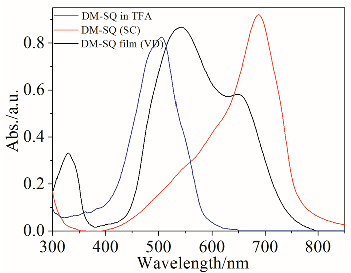
Fig. 2 shows the UV-Vis absorption spectra of DM-SQ solution (in TFA) and solid films. In TFA solvent, the dye shows a characteristical absorbance peak at 505 nm, while for the corresponding solution-deposited film (27 nm thick), a red-shifted and broadened absorption band is observed with a peak at 688 nm. The large bathochromic-shift (183 nm) could be ascribed to the formation of J-aggregates. As for the vacuum-deposited DM-SQ film (16nm thick), a much different absorption spectrum is observed with the maximum absorption at 548 nm, 43 nm red-shifted compared with the solution absorption spectrum, likely due to the formation of H-aggregates. In addition, the difference in the UV-Vis spectra between them could be partly due to the change in the conjugated degree of the dye in the solution from the interaction between the dye and the TFA solvent.
Figure 2
图 2.
DM-SQ的TFA溶液、旋涂薄膜和真空沉积薄膜的UV-Vis谱图
Figure 2.
The UV-Vis absorption spectra of the DM-SQ in TFA solution, and the DM-SQ films on quartz substrates deposited by spin-coated (SC) from TFA solution and vacuum deposition (VD)
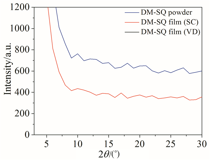
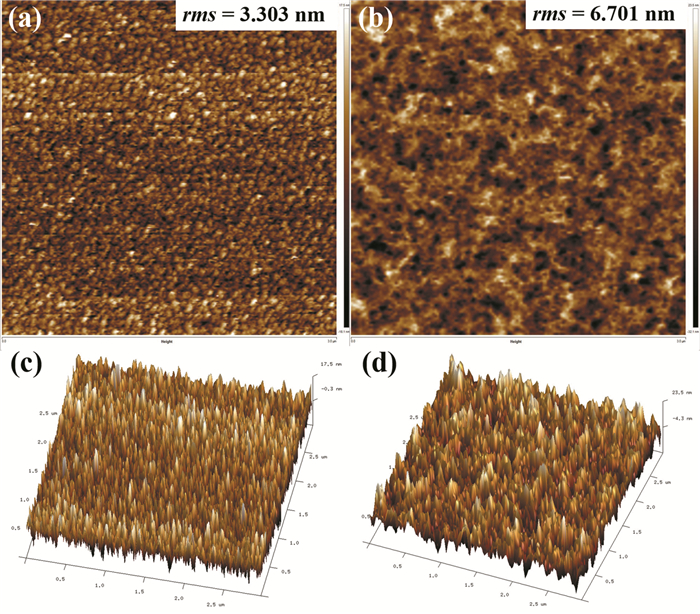
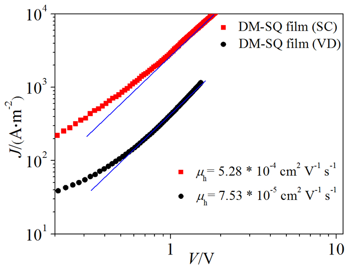
X-ray diffraction (XRD) measurements were performed for DM-SQ powder and the films prepared via solution processing and vacuum deposition, respectively. As shown in Fig. 3, the XRD spectra show similar patterns with sharp and strong diffraction peaks at 2θ ~5.34°, 10.60°, 16.02°, and 26.2° for both the powder and solution-processed film. The results indicate that DM-SQ dye is strong crystallization due to the close packing of the molecules with short methyl groups, and that the solution processing did not significantly change the crystallinity of the resultant film. The vacuum-deposited film, however, is almost amorphous state without any clear characteristic diffraction peaks. Atomic force microscopy (AFM) images (Fig. 4) indicate the formation of grain-like aggregates in the vacuum-deposited film and fibril morphology in the solution-processed film. The solution-processed film shows the root-mean-square (RMS) roughness of 6.7±0.1 nm, which is two times than that (3.3±0.1 nm) for the vacuum-deposited film, further indicating that the solution-processed film holds high crystallization as compared with the vacuum-deposited film. For the solution processed film, the fibril morphology would be beneficial to improving charge separation and charge transfer between donor and acceptor in a planar heterojunction device in the presence of these vertical channels. To gain further insights into both the films, the hole mobility was measured using the space-charge limited-current method (Fig. 5), affording values of 7.53×10⁻⁵ and 5.28×10⁻⁴ cm2 ·V-1 ·s-1 for the vacuum-deposited and solution-processed films, respectively. The solution-processed film demonstrates much higher mobility than that of the vacuum-deposited one.
Figure 3
图 3.
DM-SQ的粉末、溶液旋涂和真空沉积薄膜的XRD谱
Figure 3.
XRD patterns of DM-SQ powder and DM-SQ films deposited on quartz substrates by TFA solution coating (SC) and vacuum deposition (VD)
Figure 5.
Plots of J-V characteristic of the single hole-carrier devices based on neat film, which were estimated using the SCLC method. Blue lines represent fits of the curves using the Mott-Gurney relationship. DM-SQ (SC): the film prepared by spin-coating; DM-SQ (VD): the film prepared by vacuum deposition
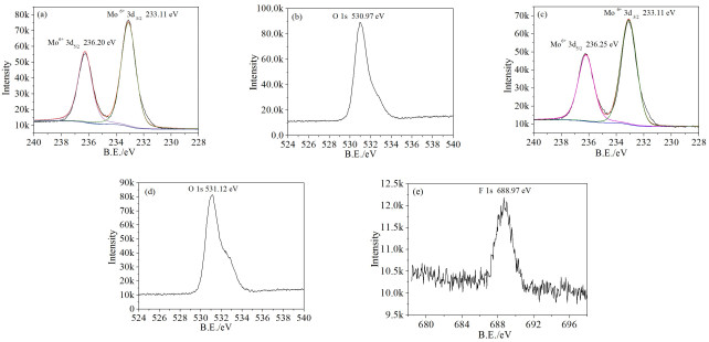
To study the photovoltaic property of DM-SQ, we chose MoOx instead of PEDOT :PSS as hole injection/extraction layers due to the corrosion of TFA to the PEDOT :PSS layer. The MoOx film was deposited by vacuum deposition, and the value of x in MoOx was estimated to be 3 by X-ray photoelectron spectroscopy (XPS) (Fig. 6).
Figure 6
图 6.
TFA处理前后MoOx层的Mo 3d和O 1s的XPS光谱:(a, b) TFA处理前MoOx层,(c~e) TFA处理后MoOx层
Figure 6.
The Mo-3d and O 1s XPS spectra of the deposited MoOx layers: (a), (b) is that before TFA treatment, the calculated Mo6+ is 100%, corresponding to MoOx with x=3; (c), (d), (e) is that after TFA treatment
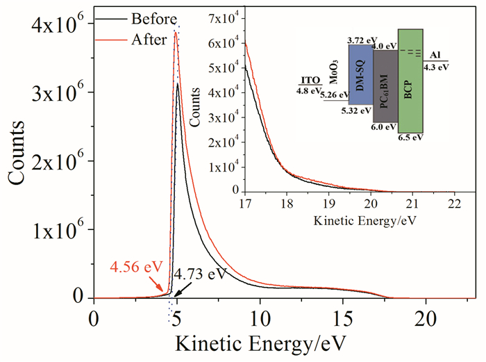
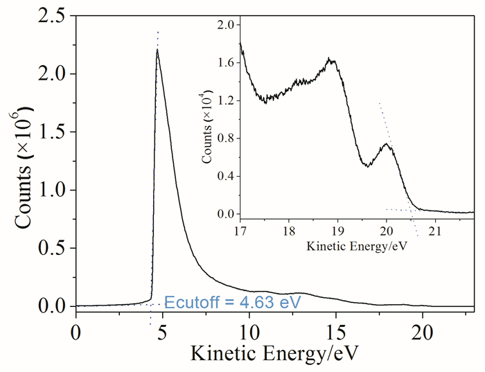
The valence band (VB) of MoO3 was determined to be -5.43 eV by the ultraviolet photoelectron spectrometer (UPS), as shown in Fig. 7. The deposited MoO3 film was treated by spin-coating pure TFA atop it and allowed for dryingTFA at ambient condition, and the XPS spectra did not show obvious changes for the Mo 3d and O 1s bands (Fig. 6). However, F 1s signal can be detected, meaning the MoO3 surface was decorated with TFA molecules. After TFA treatment, the estimated VB of the MoO3 film slightly reduced to -5.26 eV (see Fig. 7), a little higher than the VB (-5.32 eV) for the solution-processed DM-SQ pristine film, determined by UPS (Fig. 8). The LUMO level of the solution-processed DM-SQ film was estimated to be -3.72 eV from the HOMO energy and the optical band gap (Eg≈1.6 eV), estimated from the absorption spectrum of the solution-processed film. The DM-SQ LUMO energy matches that of PC61BM ([6, 6]-phenyl-C61-butyric acid methyl ester), as shown in the inset of Fig 7.
Figure 7
图 7.
TFA处理前后MoO3的UPS谱图
Figure 7.
UPS spectra of the MoO3 films before and after TFA treatment (He-I gas discharge lamp source: 21.22 eV). Insert is energy diagrams of the respective materials
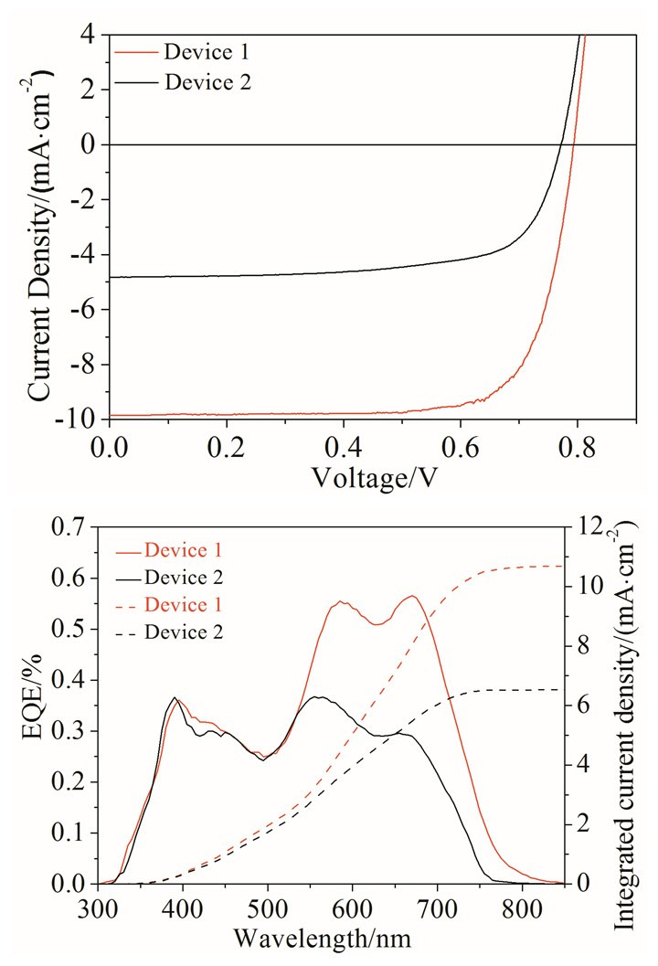
We fabricated the photovoltaic cells with the device architecture of ITO/MoO3(10 nm)/DM-SQ/PC61BM/BCP (10 nm)/Al (100 nm), as shown in Fig. 1b. Two kinds of cells were fabricated: in the case of device 1, the DM-SQ layer was fabricated via spin-coating from the TFA solution and the PC61BM layer was spin-coated atop the DM-SQ layer from the CS2 solution. Here, CS2 is selected as solvent due to its suitable solubility for PC61BM but insolubility for DM-SQ. In device 2, the DM-SQ donor layer was vacuum-deposited while the PC61BM layer was spin-coated atop the DM-SQ layer from solution. Tab. 1 lists the photovoltaic parameters of devices 1 and 2 with various thicknesses of the DM-SQ layer. The optimal solution-processed devices deliver an average short circuit photocurrent density (Jsc) of 10.84±0.21 mA ·cm-2, an average open circuit voltage (Voc) of 0.776±0.009 V, an average fill factor (FF) of 0.723±0.021, and an average power conversion efficiency (PCE) of 6.08±0.19% under the standard AM 1.5 conditions. Such efficiency represents one of the highest values reported for single-junction planar devices, while the vacuum-deposited cells gave Jsc=6.52±0.24 mA ·cm-2, Voc=0.773±0.007 V, FF=0.706±0.013, and PCE=3.56±0.22%. The corresponding (J-V) curves and EQE spectra of the devices 1 and 2 are presented in Fig. 9. For the solution-processed devices, the best performance was obtained for a 27 nm-thick DM-SQ layer, while the vacuum-deposited device 2 gave the optimal performance with a 16nm-thick DM-SQ layer. Moreover, it is clear that all the samples in the device 1 give much higher PCE values than those for the device 2 with a comparable thick DM-SQ layer. This would be associated with the fact that the solution-processed DM-SQ film holds a higher hole mobility than that of the vacuum-deposited film as indicated above. The high charge mobility guarantees effective charge transport in a relatively thick light absorbing dye layer in the device, and in turn contributes to the higher Jsc and PCE.
Table 1
表 1
不同厚度DM-SQ层的两种制备工艺器件的关键光伏指标平均值(1:溶液制备;2:真空沉积)
Table 1.
The key photovoltaic parameters of the device 1 (solution-processed) and device 2 (vacuum deposition) with a different thickness of DM-SQ layer measured under 100 mW ·cm-2 AM1.5G illumination
Fig. 9b shows the external quantum efficiency (EQE) for the 27nm-thick solution-processed device 1 and the 16nm-thick vacuum-deposited device 2. It is clear that 27 nm device 1 shows a broaden and strong spectrum response with a maximized EQE value of 62% at 690 nm, while the spectrum of the 16 nm device 2 is blue-shifted with a maximized value of only 36% at 570 nm. The values of integrated current density from the EQE spectra are 10.69 mA ·cm-2 for device 1 and 6.47 mA ·cm-2 for device 2, both of which are consistent with the values obtained from the J-V measurements.
Figure 9
图 9.
溶液制备和真空沉积最优器件的J-V曲线(a)和EQE曲线(b)
Figure 9.
(a) Representative photocurrent density-voltage (J-V) curves of the 27 nm device 1(solution-processed) and the 16nm device 2(vacuum deposition), measured under simulated AM.5G irradiation (100 mW ·cm-2). (b) External quantum efficiency (EQE) spectra for the same devices
In conclusion, we report a novel method to prepare all solution-processed planar heterojunction solar cells, in which a low soluble and strong crystalline squaraine dye (DM-SQ) was solution-processed as a donor layer by using trifluoroacetic acid solvent. The resulting DM-SQ film presents high charge mobility and allows us to use a relatively thick DM-SQ layer in the efficient solar cells, and achieve an average power conversion efficiency up to 6.08±0.19%, which is higher than that (3.56±0.22%) for the vacuum-deposited solar cells. Further work is under investigation for other crystalline organic semiconductor dyes, potentially having high change mobility but low solubility in common solvents and/or lack of high thermal stability for vacuum deposition.
[1]
(a) Mathews I, Kantareddy S N, Buonassisi T, et al. Joule, 2019, 3: 1415~1426; (b) Chen F C. Adv. Opt. Mater., 2019, 7: 1800662; (c) Reynaud C A, Clerc R, Lechene P B, et al. Sol. Energy Mater. Sol. Cells, 2019, 200: 110010; (d) Cui Y, Wang Y, Bergqvist J, et al. Nat. Energy., 2019, 5: 768~775; (e) Ding Z, Zhao R, Yu Y, et al. J. Mater. Chem. A, 2019, 7: 26533~26539; (f) Gasparini N, Salvador M, Heumueller T, et al. Adv. Energy Mater., 2017, 7: 1701561; (g) Cui Y, Yao H, Zhang J, et al. Nat. Commun., 2019, 10: 2515.
[2]
(a) Cui Y, Yao H, Hong L, et al. Natl. Sci. Rev., 2020, 7(7): 1239~1246; (b) Lin Y, Adilbekova B, Firdaus Y, et al. Adv. Mater., 2019, 31: 1902965; (c) Meng L, Zhang Y, Wan X, et al. Science, 2018, 361: 1094~1098.
[3]
(a) Keil D, Hartmann H, Moschny T. Dyes Pigm., 1991, 17: 19~27; (b) Sreejith S, Carol P, Chithra P, et al. J. Mater. Chem., 2008, 18: 264~274.
[4]
(a) Law K Y. Chem. Rev., 1993, 93: 449~486; (b) Law K Y, Bailey F C. J. Org. Chem., 1992, 57: 3278~3286; (c) Law K Y. J. Phys. Chem., 1987, 91: 5184~5193.
[5]
Chen C T, Marder S R, Cheng L T. J. Chem. Soc., Chem. Commun., 1994: 259~260.
[6]
(a) Chen C T, Marder S R, Cheng L T. J. Am. Chem. Soc., 1994, 116: 3117~3118; (b) Beverina L, Crippa M, Salice P, et al. Chem. Mater., 2008, 20: 3242~3244.
[7]
Chen G, Sasabe H, Igarashi T, et al. J. Mater. Chem. A, 2015, 3: 14517~14534
[8]
(a) Wang S, Mayo E I, Perez M D, et al. Appl. Phys. Lett., 2009, 94: 233304; (b) Wei G, Lunt R R, Sun K, et al. Nano Lett., 2010, 10: 3555~3559; (c) Wei G D, Wang S, Renshaw K, et al. ACS Nano, 2010, 4: 1927~1934; (d) Wei G, Wang S, Sun K, et al. Adv. Energy Mater., 2011, 1: 184~187; (e) Wei G, Xiao X, Wang S, et al. Nano Lett., 2011, 11: 4261~4264; (f) Chen G, Sasabe H, Wang Z, et al. Phys. Chem. Chem. Phys., 2012, 14: 14661~14666; (g) Chen G, Yokoyama D, Sasabe H, et al. Appl. Phys. Lett., 2012, 101: 083904; (h) Wei G, Xiao X, Wang S, et al. ACS Nano, 2012, 6: 972~978; (i) Xiao X, Wei G, Wang S, et al. Adv. Mater., 2012, 24: 1956~1960; (j) Zimmerman J D, Lassiter B E, Xiao X, et al. ACS Nano, 2013, 7: 9268~9275; (k) Chen G, Sasabe H, Lu W, et al. J. Mater. Chem. C, 2013, 1: 6547~6552. (l) Sasabe H, Igrashi T, Sasaki Y, et al. RSC Adv., 2014, 4: 42804~42807; (m) Karak S, Homnick P J, Pelle A M D, et al. ACS Appl. Mater. Interf., 2014, 6: 11376~11384; (n) Chen G, Sasabe H, Sasaki Y, et al. Chem. Mater., 2014, 26: 1356~1364.
[9]
(a) Kang I, Yun H J, Chung D S, et al. J. Am. Chem. Soc., 2013, 135: 14896~14899; (b) Kang B, Kim R, Lee S B, et al. J. Am. Chem. Soc., 2016, 138: 3679~3686.
[10]
Law K Y, Facci J S, Bailey F C, et al. J. Imaging Sci., 1990, 34: 31.
[11]
Schena A, Johnsson K. Angew. Chem. Int. Ed., 2014, 53: 1302~1305.
[12]
Yan Z, Guang S, Xu H, et al. RSC Adv., 2013, 3: 8021~8027.
[13]
Dacuna J, Salleo A. Phys. Rev. B, 2011, 84: 195209.
Figure 1
a) The chemical structure of the DM-SQ dye; (b) Device schematic of the bilayer PHJ solar cell
Figure 2
The UV-Vis absorption spectra of the DM-SQ in TFA solution, and the DM-SQ films on quartz substrates deposited by spin-coated (SC) from TFA solution and vacuum deposition (VD)
Figure 5
Plots of J-V characteristic of the single hole-carrier devices based on neat film, which were estimated using the SCLC method. Blue lines represent fits of the curves using the Mott-Gurney relationship. DM-SQ (SC): the film prepared by spin-coating; DM-SQ (VD): the film prepared by vacuum deposition
Figure 6
The Mo-3d and O 1s XPS spectra of the deposited MoOx layers: (a), (b) is that before TFA treatment, the calculated Mo6+ is 100%, corresponding to MoOx with x=3; (c), (d), (e) is that after TFA treatment
Figure 7
UPS spectra of the MoO3 films before and after TFA treatment (He-I gas discharge lamp source: 21.22 eV). Insert is energy diagrams of the respective materials
Figure 9
(a) Representative photocurrent density-voltage (J-V) curves of the 27 nm device 1(solution-processed) and the 16nm device 2(vacuum deposition), measured under simulated AM.5G irradiation (100 mW ·cm-2). (b) External quantum efficiency (EQE) spectra for the same devices
Table 1.
The key photovoltaic parameters of the device 1 (solution-processed) and device 2 (vacuum deposition) with a different thickness of DM-SQ layer measured under 100 mW ·cm-2 AM1.5G illumination

 下载:
下载:

 下载:
下载:


