Morphology Engineering toward Highly Emissive Mn2+ Doped PEA2PbBr4 Perovskite with Their LED Application via Phosphonium Passivation
English
Morphology Engineering toward Highly Emissive Mn2+ Doped PEA2PbBr4 Perovskite with Their LED Application via Phosphonium Passivation
-
Key words:
- 2D perovskite
- / Mn2+ doped
- / energy transfer
- / perovskite LED
-
INTRODUCTION
Lead halide perovskite is extensively explored in various opt-electric devices due to its excellent photoelectric properties.[1-3] In particular, a large number of attempts have been made on perovskite light-emitting diodes (Pe-LED) owing to their adjustable bandgap, high color purity and low cost.[4-8] So far, highly efficient Pe-LEDs with EQE over 20% have been reported via morphology control, solvent engineering, organic molecular passivation, and so on.[9-11] While, the environmental stability and toxicity of lead are still great challenges for their further practical application.
Dimensionality reduction from molecular and morphology levels is an effective method to improve the stability of perovskite.[12-20] While the A-site cation is large enough, 3D perovskite could not extend but be separated by interlayer to form 2D quantum wells (QWs), [21, 22] in which both sides of metal halides in 2D quantum wells are surrounded by organic ligands with π-π stacking, giving a better stable phase.[23] Quasi 2D mutiquantum wells (n > 2) usually have excellent luminescence properties due to the cascade energy transfer from low- to high-order phase, [24] while field-induced decomposition of spacer cations, excessive local carrier concentration and strong Auger recombination caused by the efficient energy transfer are the crucial factors affecting the stability and lifetime of quasi-2D PeLEDs.[25, 26] For pure 2D perovskite with n = 1, fast exciton quenching at room temperature and their high trap density usually result in an extremely-low photoluminescence quantum yield (PLQY < 1%).[25, 27-29] Introducing photoactive heteroatoms, such as Eu2+, Mn2+, etc. into the lattice of 2D perovskite as energy receptors, is an effective way to improve the luminescence properties.[30-35] Related attempts have been made on their photoluminescence property, however, only a small part of these doped materials can be employed as electroluminescence devices and the corresponding device features with a low external quantum efficiency (EQE) and brightness due to their poor energy transfer efficiency.[36, 37]
In addition, reduction of particle size via morphology modification provides an efficient approach toward highly emissive perovskite.[38-41] For instance, bulk 3D perovskites usually have a small exciton binding energy and low photoluminescence quantum yield. In contrast, perovskite quantum dots or nanocrystals exhibit excellent photoluminescence as the strong quantum confinement effect will greatly improve the efficiency of radiation recombination.[42, 43] However, the routine prepared nanocrystals (NCs) suffer from inferior stability and low emission efficiency during the film formation as a result of the capping ligand dissociation and particle aggregation. In-situ formation of perovskite nanocrystals (NCs) by solution processing of the blend of perovskite precursor and polymer/organic molecular could overcome the issues mentioned above and has been widely used in 3D perovskite.[44-46] Due to the similar electronic structure of phosphine and amine, phosphonium can effectively participate in the crystallization process of perovskite and realize efficient in-situ passivation, [47, 48] while their attempts on 2D perovskite are rarely reported.
In this work, we report a highly emissive Mn2+ doped 2D PEA2PbBr4 perovskite thin film by introducing 9-fluorenyl triphenylphosphonium bromide (Scheme S1) with poor solubility in DMF (60 mg/mL at room temperature). The as-prepared film has bright orange emission peaked at 600 nm with the PLQY as high as 73.73% at room temperature, which is about 1.3 times higher than that of pristine Mn2+ doped 2D PEA2PbBr4 perovskite thin film. Electroluminescent devices using phophonium passivated thin films as active layer exhibit a brightness of 430.8 cd/m2 and an external quantum efficiency of 0.12%, which is a great improvement over that for the device based on the pristine film. The characterization of photophysical property and morphology demonstrates that enhanced confinement effect and smoother surface induced by smaller crystalline size together with highly efficient energy transfer and radiative recombination are responsible for the enhanced luminescent performance. This is the first report on in-situ passivation of low-dimensional hybrids, and this work proposes a feasible idea for regulating energy transfer from the perspective of morphology engineering.
RESULT AND DISCUSSION
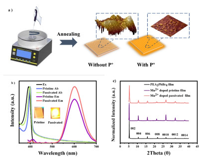
As shown in Figure 1a, Mn2+ doped PEA2PbBr4 (VPb2+: VMn2+ = 2:1) and phosphonium passivated Mn2+ doped PEA2PbBr4 (VPb2+: VMn2+ = 2:1) films were prepared by spin-coating dimethylformamide solutions containing perovskite precursors with/without phosphonium salt. The real mass ratio of Mn2+: Pb2+ was determined to be 29.3:70.7 by X-ray Fluorescence Spectrometer (XRF), as shown in Table S2. The 2D PEA2PbBr4 thin film was also prepared as a control following the same procedure. The crystallization of 2D perovskite can be identified from PXRD patterns (Figure 1c). Within the diffraction angle of 5-40°, both pristine and phosphonium passivated films exhibit periodic diffraction peaks with regular spacing, similar to those of previously reported 2D PEA2PbBr4.[49] No additional peaks appear in Mn2+ doped PEA2PbBr4 films, indicating the formation of uniform alloyed crystalline. Furthermore, the broadening of these diffraction peaks after passivation implies the formation of small-size nanocrystals (NCs). Debye-Scherrer equation (1) is used to estimate the grain size ()[50], where is a dimensionless shape factor, is the X-ray wavelength, is the line broadening at half of the maximum intensity and is the Bragg angle. From the diffraction peaks, the average grain size on the pristine film is calculated to be 43.1 nm, while that of the passivated film is only 26.2 nm, which is only 60% of that before passivation (Table S3). To our knowledge, this is the first in-situ passivation attempt for low-dimensional hybrids.
$ D=\frac{K\gamma }{B\mathrm{cos}\theta } $ (1) Figure 1
Figure 1. a) Schematic illustration of the fabrication of pristine and in-site passivated perovskite thin films. (Illustration is 3D AFM images) b) UV-Vis absorption, photoluminescence excitation (PLE) and emission (PL) spectra of pristine and in-site passivated perovskite thin films. The illustration shows the film photos before and after passivation. c) Powder X-ray diffraction patterns (PXRD) of PEA2PbBr4, the pristine and in-site passivated films.Their photophysical properties are investigated as shown in Figure 1b and Figure S1. The PLE of the two samples is almost the same. A strong and characteristic exciton absorption at 394 nm and the maximum emission located at 413 nm with a full width at half height (FWHM) of 14 nm were observed for pure 2D PEA2PbBr4 film. The small Stokes shift suggests that the luminescence comes from the exciton recombination of quantum wells (QWs), which is similar to the previous report.[51] The photoluminescence quantum yield of the film at room temperature is determined as 0.84% using an integrated sphere (Figure S3). The low quantum yield limits its application as a luminescent material, while their violet narrow-band emission characteristics and the intrinsic wide-bandgap make it a good candidate as the donor of energy transfer to realize high-efficiency luminescence. After Mn2+ doped as an energy acceptor, except the violet emission of 2D PEA2PbBr4, a new broad emission appears at 600 nm (FWHM = 78 nm) with PLQY of 58.92% and an average lifetime of 0.47 ms (Figure S5, S6). The orange emission along with millisecond lifetime demonstrates that emission is originated from the 4T1 → 6A1 transition of Mn2+ in octahedron environment. Furthermore, (9-fluorenyl) triphenylphosphorus bromide with poor solubility in DMF was introduced to Mn2+ doped 2D perovskite film. Due to the strong electrostatic interaction between phosphonium and halogen, and differential crystallization rates of 2D perovskites and phosphonium, the phosphonium could act as an organic matrix and separate the crystallization process of perovskite and finally induce the formation of uniform perovskite nanocrystals (NCs) film.[52] In the in-situ formed NCs film, both the absorption and emission from 2D PEA2PbBr4 experienced a decline in intensity and a peak blue-shift with absorption shifted from 403 to 398 nm and emission from 413 to 408 nm. Instead, the emission intensity from Mn2+ increased with the PLQY reached to 73.73% (Figure S9), which is about 1.3 times higher than that of the film before passivation. The average lifetime is determined as 0.57 ms (Figure S8), matching well with the improved luminescence efficiency. It is reasonable as the reduced size could increase the exciton binding energy and improve the radiative recombination.
To calculate the energy transfer efficiency (
$ {\phi }_{ET} $ ) from 2D PEA2PbBr4 quantum well to Mn2+ emission center, the fluorescence lifetime of violet emission in pure 2D PEA2PbBr4, Mn2+ doped 2D PEA2PbBr4 and phosphonium passivated Mn2+ doped 2D PEA2PbBr4 were collected (Figure S2, S4 and S7) and fitted with formulas (2)-(4).[53-55]$ {t}_{0}=\frac{1}{{k}_{ex-r}+{k}_{ex-nr}} $ (2) $ {t}_{1}=\frac{1}{{k}_{ex-r}+{k}_{ex-nr}+{k}_{ET}} $ (3) $ {\phi }_{ET}=\frac{{k}_{ET}}{{k}_{ex-r}+{k}_{ex-nr}+{k}_{ET}} $ (4) The energy transfer efficiency was calculated as 58.23% for Mn2+ doped 2D PEA2PbBr4 and the efficiency boosted to 74.68% for phosphonium passivated one, in good agreement with our results.
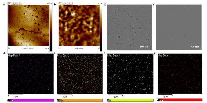
To better understand why the phosphonium passivated film has enhanced luminescence efficiency, the film morphology was investigated by AFM and SEM. As shown in Figure 2a and b, large pinholes were randomly dispersed on the surface on the Mn2+ doped 2D PEA2PbBr4 with roughness (Rq) of 26.4 nm. While a better smooth film was observed on phosphonium passivated film with Rq decreasing dramatically to 4.85 nm (Figure S13 and S14). The SEM images show good agreement with the observation from AFM images. The pristine film has lower coverage and much more surface defects, while the film becomes denser and more uniform after phosphonium passivation (Figure 2c, d). Besides, the Energy dispersive X-ray spectroscopy (EDS) (Figure 2e-h) shows a very uniform distribution of phosphorus, bromine, lead and manganese.
Figure 2
FT-IR and 31P-NMR were used to explore the passivation mechanism (Figure S15 and S16). The chemical shift of 31P-NMR shifts to high field as the shielding effect is enhanced when the phosphonium interacts with PbBr6 octahedra. FT-IR shows the characteristic peaks of PbBr2 at 740, 1378 and 1466 cm-1 and MnBr2 at about 1515 cm-1 are significantly enhanced after passivation by phosphonium, indicating higher crystallinity. Besides, a new peak appears in the fingerprint area at 1182 cm-1, indicating that phos-phonium does not physically adhere to the surface of PEA2PbBr4, but forms a passivation layer via cation exchange with PEA+.[48]
The above results show the participation of phosphonium in the crystallization process plays a great role in morphology regulation. And the as-formed smaller size particle with high surface coverage and uniform spatial distribution of Mn2+ ions could enhance the confinement effect and facilitate efficient energy transfer between 2D perovskite and Mn2+, thus achieving better photoluminescence and electroluminescence.
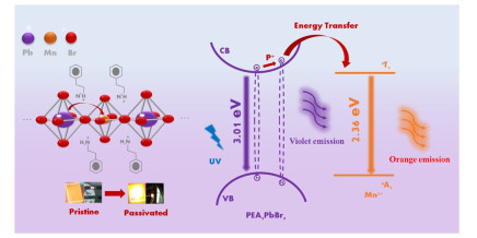
To sum up, a feasible strategy to regulate energy transfer and luminescence performance from the morphology is proposed (Scheme 1). Under UV light excitation, excitons formed upon the electrons of PEA2PbBr4 transited from valence band (VB) to conduction band (CB). After the introduction of 9-fluorenyl triphenylphosphonium bromide, smaller crystals are formed in situ through the separation of crystallization process, resulting in high exciton binding energy due to the enhanced confinement effect of smaller size, which in further facilitate excitons transferred to 4T1 excited states of Mn2+ via Dexter pathway and then decayed to the 6A1 ground state accompanied with orange emission.
Scheme 1
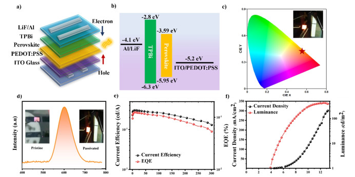
Inspired by the ultra-high PLQY and uniform and smooth surface, the solution-processed LED based on Mn2+ doped PEA2PbBr4 NCs film was prepared with device structure of ITO/PEDOT: PSS/Perovskite/TPBi/LiF/Al (Figure 3a). The PEDOT: PSS and TPBi were used as hole-injection and electron transporting layers, respectively. For comparison, a control device was fabricated in the same way using none-passivated film. As shown in Figure 3b and c, the electroluminescence spectrum remains unchanged before and after phosphonium passivation with EL peak located at 600 nm and a CIE coordinate at (0.5612, 0.4138), which is identical to their photoluminescence emission. Besides, the violet emission from 2D PEA2PbBr4 almost disappeared, indicating complete energy-transfer from 2D quantum wells to Mn2+.
Figure 3
Figure 3. a) LED architecture. b) Schematic diagram of LED device energy structure, and relevant energy levels are obtained through UPS valence band spectrum (Figure S12 and Table S1) and literature. c) Electroluminescence CIE coordinate diagram of LED device. d) Electroluminescence spectrum and lighting photos of LED devices. e) CE-J-EQE curve of LED device based on in-situ passivated film. f) J-V-L curve of LED device based on in-situ passivated film.The relevant parameters of device efficiency are shown in Figure 3d, e and Figure S10, S11. The LED device prepared based on Mn2+ doped PEA2PbBr4 film has a turn-on voltage of 5 V, a maximum brightness of 29.9 cd/m2, a maximum current efficiency of 0.004 cd/A and an external quantum efficiency (EQE) of 0.0017%. The optimal EQE is close to the efficiency of existing LED devices based on Mn2+ doped PEA2PbBr4[36], and slightly lower than that of previously reported pure PEA2PbBr4 polycrystalline film with EQE of 0.002%, [56] which may be attributed to the exciton loss in the energy transfer process. In contrast, an obviously reduced turn-on voltage was observed for phosphonium passivated film with Von of 3.9 V, which mostly results from improved film coverage and thus lower current leakage. Moreover, significant improvement of device performance was achieved after passivation. The maximum brightness is 430.8 cd/m2, which is 14-fold higher than that of control device. The maximum EQE of 0.12% was obtained, which represents a huge improvement over that for the device based on the pristine film. The better electron and hole confinement and improved film morphology account for the enhancement of device performance. For 2D organic-inorganic hybrid perovskite, in-situ passivation is still an effective way to improve the efficiency of devices.
CONCLUSION
In conclusion, a Mn2+ doped PEA2PbBr4 nanocrystals (NCs) film with orange emission is reported by introducing organic ligands with poor solubility in the precursor solution. The as-prepared film has smaller crystal size and higher PLQY. Pe-LEDs were fabricated based on the pristine and 9-fluorenyl triphenylphosphonium bromide passivated films. A huge improvement in the maximum EQE and a 14-fold improvement in the maximum brightness were observed for the passivated film. Characterization of photophysical properties demonstrates that the improvement of luminescence performance mostly results from the enhanced confinement effect with smaller size, and thus highly efficient energy transfer and radiative recombination. This is the first report on in-situ passivation of 2D organic-inorganic hybrid perovskite, and this work proposes a feasible idea of regulating energy transfer from the perspective of morphology.
EXPERIMENT
Chemicals and Reagents. Phenylethylamine (C8H11N, 98%) was obtained from Energy-chemical (China). PEDOT: PSS 4083(5-6%), 1, 3, 5-tris(1-phenyl-1H-benzimidazol-2-yl) benzene (TPBi), lithium fluoride (LiF) and Lead (Ⅱ) bromide (PbBr2, 99.9%) were obtained from Xi'an Polymer Light Technology Corp (China). Manganous (Ⅱ) bromide (MnBr2, 99%) and 9-fluorenyl triphenylphosphonium bromide (C31H24P+Br-, 97%) were purchased from Alfa Aesar (USA). The patterned Indium Tinoxide (ITO) glasses were bought from Ying Kou You Xuan Trade Co., Ltd (China). The solvents for photophysical measurements and device fabrication are of spectroscopic grade.
Preparation of the Mn2+ Doped PEA2PbBr4 in-situ Nanocrystals (NCs) Film. The perovskite precursor was prepared by mixing PEA2PbBr4 (100 mg/mL) and PEA2MnBr4 (100 mg/mL) with appropriate ratio in N, N-dimethylformamide (DMF). Then, different amounts of 9-fluorenyl triphenylphosphonium bromide were added to the mixed solution and heated at 120 ℃ for 5 minutes. Tetraphenyl phosphine bromide and 3-carbazole triphenyl phosphine bromide were also used to prepare the precursor as control experiment. The light-emitting film was formed using the spin-coating method at 3800 rpm for 30 s in a nitrogen-filled glove box after the precursor cooling to room temperature. The samples were then annealed on a hot plate at 70 ℃ for 15 min. After screening the ratio of phosphonium, Mn2+ and Pb2+, the brightest film can be obtained by mixing Mn2+ and Pb2+ in the precursor in the volume ratio of 1:2 with 80 mg/mL phosphonium. The test and characterization in this paper were carried out according to this ratio. (The screening process is shown in the Figure S17-19)
Device Fabrication. ITO substrates were cleaned by detergent and deionized water, then successively washed by ethanol, acetone and isopropanol under ultrasonic, respectively, followed by UV-O3 treatment for 15 min. A PEDOT: PSS solution was spin-coated on the ITO substrates at 4800 r/min for 50 s, which was then dried at 140 ℃ for 20 min. The emitting layers were prepared by the above method. Subsequently, TPBi (28 nm, 0.3 nm/s), LiF (1.3 nm, 0.05 nm/s) and Al (110 nm, 3 nm/s) were thermally evaporated in a vacuum chamber at a base pressure lower than 4.0×10⁻⁴ Pa. The current density voltage brightness (I-V-B) characteristics of the devices were measured on a Keithley 2400/2000 source meter with a calibrated silicon photodiode. All the measurements of the devices were performed under dry and ambient conditions with humidity lower than 30%.
Characterization. The UV-Vis absorption spectra were conducted on a Perkin-Elmer Lambda 950 UV-Vis spectrophotometer. The photoluminescent properties were measured on an FLS920 Edinburgh fluorescence spectrometer. The PXRD patterns were recorded on Rigaku Miniflex 600 with Cu Kα (λ = 1.54184 Å) radiation. The electroluminescence spectra were recorded on the Ocean optical spectrometer. The appearance of the films was determined by atomic force microscopy (AFM) (Bruker DIMENSION ICON) and scanning electron microscope (SEM) (Zeiss Sigma 300). Ultraviolet photoelectron spectra (UPS) were recorded on a Thermo Scientific Escalab 250 Xi instrument using monochromatic Al Kα radiation (hν = 1486.7 eV). Fluorescence Spectrometer (XRF) was measured in ZSX PrimusIII+.
ACKNOWLEDGEMENTS: This work was supported by the National Natural Science Foundation of China (Grants 22175181 and 92061202), the Fujian Science and Technology Project (Grant 2020L3022), and the Strategic Priority Research Program of Chinese Academy of Sciences (Grant XDB20000000). The authors declare no competing interests.
COMPETING INTERESTS
Supplementary information is available for this paper at http://manu30.magtech.com.cn/jghx/EN/10.14102/j.cnki.0254-5861.2022-0088
ADDITIONAL INFORMATION
For submission: https://mc03.manuscriptcentral.com/cjsc
-
-
[1]
Wu, J. M.; Wang, L. X.; Feng, A. B.; Yang, S.; Li, N.; Jiang, X. M.; Liu, N. A. Q.; Xie, S. D.; Guo, X. B.; Fang, Y. J. Self-powered FA(0.55)MA(0.45)PbI(3) single-crystal perovskite X-ray detectors with high sensitivity. Adv. Funct. Mater. 2022, 32, 2109149. doi: 10.1002/adfm.202109149
-
[2]
Green, M. A.; Ho-Baillie, A. Perovskite solar cells: the birth of a new era in photovoltaics. Acs Energy Lett. 2017, 2, 822-830. doi: 10.1021/acsenergylett.7b00137
-
[3]
Li, N.; Feng, A. B.; Guo, X. B.; Wu, J. M.; Xie, S. D.; Lin, Q. L.; Jiang, X. M.; Liu, Y.; Chen, Z. L.; Tao, X. T. Engineering the hole extraction interface enables single-crystal MAPbI3 perovskite solar cells with efficiency exceeding 22% and superior indoor response. Adv. Energy Mater. 2022, 12, 2103241. doi: 10.1002/aenm.202103241
-
[4]
Stranks, S. D.; Eperon, G. E.; Grancini, G.; Menelaou, C.; Alcocer, M. J. P.; Leijtens, T.; Herz, L. M.; Petrozza, A.; Snaith, H. J. Electron-hole diffusion lengths exceeding 1 micrometer in an organometal trihalide perovskite absorber. Science 2013, 342, 341-344. doi: 10.1126/science.1243982
-
[5]
Snaith, H. J. Perovskites: the emergence of a new era for low-cost, high-efficiency solar cells. J. Phys. Chem. Lett. 2013, 4, 3623-3630. doi: 10.1021/jz4020162
-
[6]
De Wolf, S.; Holovsky, J.; Moon, S. J.; Loper, P.; Niesen, B.; Ledinsky, M.; Haug, F. J.; Yum, J. H.; Ballif, C. Organometallic halide perovskites: sharp optical absorption edge and its relation to photovoltaic performance. J. Phys. Chem. Lett. 2014, 5, 1035-1039. doi: 10.1021/jz500279b
-
[7]
Unger, E. L.; Kegelmann, L.; Suchan, K.; Sorell, D.; Korte, L.; Albrecht, S. Roadmap and roadblocks for the bandgap tunability of metal halide perovskites. J. Mater. Chem. A 2017, 5, 15983-15983. doi: 10.1039/C7TA90141K
-
[8]
Sutton, R. J.; Eperon, G. E.; Miranda, L.; Parrott, E. S.; Kamino, B. A.; Patel, J. B.; Horantner, M. T.; Johnston, M. B.; Haghighirad, A. A.; Moore, D. T. Bandgap-tunable cesium lead halide perovskites with high thermal stability for efficient solar cells. Adv. Energy Mater. 2016, 6, 1502458. doi: 10.1002/aenm.201502458
-
[9]
Lin, K. B.; Xing, J.; Quan, L. N.; de Arquer, F. P. G.; Gong, X. W.; Lu, J. X.; Xie, L. Q.; Zhao, W. J.; Zhang, D.; Yan, C. Z. Perovskite light-emitting diodes with external quantum efficiency exceeding 20 percent. Nature 2018, 562, 245-248. doi: 10.1038/s41586-018-0575-3
-
[10]
Ma, D. X.; Lin, K. B.; Dong, Y. T.; Choubisa, H.; Proppe, A. H.; Wu, D.; Wang, Y. K.; Chen, B.; Li, P. C.; Fan, J. Z. Distribution control enables efficient reduced-dimensional perovskite LEDs. Nature 2021, 599, 594-598. doi: 10.1038/s41586-021-03997-z
-
[11]
Fang, Z. B.; Chen, W. J.; Shi, Y. L.; Zhao, J.; Chu, S. L.; Zhang, J.; Xiao, Z. G. Dual passivation of perovskite defects for light-emitting diodes with external quantum efficiency exceeding 20%. Adv. Funct. Mater. 2020, 30, 1909754. doi: 10.1002/adfm.201909754
-
[12]
Meng, Z.; Guo, D. P.; Yu, J. G.; Fan, K. Investigation of Al2O3 and ZrO2 spacer layers for fully printable and hole-conductor-free mesoscopic perovskite solar cells. Appl. Surf. Sci. 2018, 430, 632-638. doi: 10.1016/j.apsusc.2017.05.018
-
[13]
Zhang, Y.; Li, F. Z.; Jiang, K. J.; Huang, J. H.; Wang, H. J.; Fan, H. C.; Wang, P. C.; Liu, C. M.; Zhang, L. P.; Song, Y. L. From 2D to 3D: a facile and effective procedure for fabrication of planar CH3NH3PbI3 perovskite solar cells. J. Mater. Chem. A 2018, 6, 17867-17873. doi: 10.1039/C8TA07048B
-
[14]
Roghabadi, F. A.; Alidaei, M.; Mousavi, S. M.; Ashjari, T.; Tehrani, A. S.; Ahmadi, V.; Sadrameli, S. M. Stability progress of perovskite solar cells dependent on the crystalline structure: from 3D ABX3 to 2D Ruddlesden-Popper perovskite absorbers. J. Mater. Chem. A 2019, 7, 5898-5933. doi: 10.1039/C8TA10444A
-
[15]
Li, G.; Zhang, T. Y.; Guo, N. J.; Xu, F.; Qian, X. F.; Zhao, Y. X. Ion-exchange-induced 2D-3D conversion of HMA(1-x)FA(x)PbI(3)Cl perovskite into a high-quality MA(1-x)FA(x)PbI(3) perovskite. Angew. Chem. Int. Ed. 2016, 55, 13460-13464. doi: 10.1002/anie.201606801
-
[16]
Guo, D. P.; Yu, J. G.; Fan, K.; Zou, H. Y.; He, B. W. Nanosheet-based printable perovskite solar cells. Sol. Energ. Mat. Sol. C 2017, 159, 518-525. doi: 10.1016/j.solmat.2016.09.043
-
[17]
Chang, S. H.; Huang, W. C.; Chen, C. C.; Chen, S. H.; Wu, C. G. Effects of anti-solvent (iodobenzene) volume on the formation of CH3NH3PbI3 thin films and their application in photovoltaic cells. Appl. Surf. Sci. 2018, 445, 24-29. doi: 10.1016/j.apsusc.2018.03.123
-
[18]
Lan, C. Y.; Zhou, Z. Y.; Wei, R. J.; Ho, J. C. Two-dimensional perovskite materials: from synthesis to energy-related applications. Mater. Today Energy 2019, 11, 61-82. doi: 10.1016/j.mtener.2018.10.008
-
[19]
Gu, H.; Chen, S. C.; Zheng, Q. D. Long-term stable 2D Dion-Jacobson phase perovskite photodiode with low dark current and high on/off ratio. Chin. J. Struct. Chem. 2021, 40, 1621-1630.
-
[20]
Zhang, J. H.; Zhou, S. H.; Lin, H. Dimensionality reducing from three-dimensional RbLu5Te8 to two-dimensional CsMnGdTe3: syntheses, crystal and electronic structures. Chin. J. Struct. Chem. 2020, 39, 1770-1780.
-
[21]
Dou, L. T. Emerging two-dimensional halide perovskite nanomaterials. J. Mater. Chem. C 2017, 5, 11165-11173. doi: 10.1039/C7TC02863F
-
[22]
Saparov, B.; Mitzi, D. B. Organic-inorganic perovskites: structural versatility for functional materials design. Chem. Rev. 2016, 116, 4558-4596. doi: 10.1021/acs.chemrev.5b00715
-
[23]
Ajayakumar, A.; Muthu, C. V.; Dev, A.; Pious, J. K.; Vijayakumar, C. Two-dimensional halide perovskites: approaches to improve optoelectronic properties. Chem. -Asian J. 2022, 17, e202101075.
-
[24]
Yuan, M. J.; Quan, L. N.; Comin, R.; Walters, G.; Sabatini, R.; Voznyy, O.; Hoogland, S.; Zhao, Y. B.; Beauregard, E. M.; Kanjanaboos, P. Perovskite energy funnels for efficient light-emitting diodes. Nat. Nanotechnol. 2016, 11, 872-875. doi: 10.1038/nnano.2016.110
-
[25]
Jiang, Y. Z.; Cui, M. H.; Li, S. S.; Sun, C. J.; Huang, Y. M.; Wei, J. L.; Zhang, L.; Lv, M.; Qin, C. C.; Liu, Y. F. Reducing the impact of Auger recombination in quasi-2D perovskite light-emitting diodes. Nat. Commun. 2021, 12, 1-10. doi: 10.1038/s41467-020-20314-w
-
[26]
Zhang, L.; Sun, C. J.; He, T. W.; Jiang, Y. Z.; Wei, J. L.; Huang, Y. M.; Yuan, M. J. High-performance quasi-2D perovskite light-emitting diodes: from materials to devices. Light-Sci. Appl. 2021, 10, 1-26. doi: 10.1038/s41377-020-00435-z
-
[27]
Hong, X.; Ishihara, T.; Nurmikko, A. V. Dielectric confinement effect on excitons in PbI4-based layered semiconductors. Phys. Rev. B 1992, 45, 6961-6964. doi: 10.1103/PhysRevB.45.6961
-
[28]
Chong, W. K.; Thirumal, K.; Giovanni, D.; Goh, T. W.; Liu, X. F.; Mathews, N.; Mhaisalkar, S.; Sum, T. C. Dominant factors limiting the optical gain in layered two-dimensional halide perovskite thin films. Phys. Chem. Chem. Phys. 2016, 18, 14701-14708. doi: 10.1039/C6CP01955B
-
[29]
Gauthron, K.; Lauret, J. S.; Doyennette, L.; Lanty, G.; Al Choueiry, A.; Zhang, S. J.; Brehier, A.; Largeau, L.; Mauguin, O.; Bloch, J. Optical spectroscopy of two-dimensional layered (C6H5C2H4-NH3)(2)-PbI4 perovskite. Opt. Express. 2010, 18, 5912-5919. doi: 10.1364/OE.18.005912
-
[30]
Bakthavatsalam, R.; Biswas, A.; Chakali, M.; Bangal, P. R.; Kore, B. P.; Kundu, J. Temperature-dependent photoluminescence and energy-transfer dynamics in Mn2+-doped (C4H9NH3)(2)PbBr4 two-dimensional (2D) layered perovskite. J. Phys. Chem. C 2019, 123, 4739-4748. doi: 10.1021/acs.jpcc.9b00207
-
[31]
Zhou, G. J.; Jiang, X. X.; Molokeev, M.; Lin, Z. S.; Zhao, J.; Wang, J.; Xia, Z. G. Optically modulated ultra-broad-band warm white emission in Mn2+-doped (C6H18N2O2)PbBr4 hybrid metal halide phosphor. Chem. Mater. 2019, 31, 5788-5795. doi: 10.1021/acs.chemmater.9b01864
-
[32]
Dutta, S. K.; Dutta, A.; Das Adhikari, S.; Pradhan, N. Doping Mn2+ in single-crystalline layered perovskite microcrystals. Acs Energy Lett. 2019, 4, 343-351. doi: 10.1021/acsenergylett.8b02349
-
[33]
Zhou, G. J.; Jia, X. F.; Guo, S. Q.; Molokeev, M.; Zhang, J. Y.; Xia, Z. G. Role of halogen atoms on high-efficiency Mn2+ emission in two-dimensional hybrid perovskites. J. Phys. Chem. Lett. 2019, 10, 4706-4712. doi: 10.1021/acs.jpclett.9b01996
-
[34]
Su, B. B.; Molokeev, M. S.; Xia, Z. G. Unveiling Mn2+ dopant states in two-dimensional halide perovskite toward highly efficient photoluminescence. J. Phys. Chem. Lett. 2020, 11, 2510-2517. doi: 10.1021/acs.jpclett.0c00593
-
[35]
Wang, B.; Mu, T. H.; Ling, J. R.; Zhou, Y. F.; Xu, W. T.; Lin, H. Doping effect of Bi3+ on the properties of YAG: Ce3+, Mn2+ phosphor ceramics for warm WLEDs. Chin. J. Struct. Chem. 2020, 39, 511-518.
-
[36]
Cortecchia, D.; Mroz, W.; Neutzner, S.; Borzda, T.; Folpini, G.; Brescia, R.; Petrozza, A. Defect engineering in 2D perovskite by Mn(Ⅱ) doping for light-emitting applications. Chem-Us. 2019, 5, 2146-2158. doi: 10.1016/j.chempr.2019.05.018
-
[37]
Zhang, H. H.; Yao, J. N. A.; Yang, Y. A.; Fu, H. B. Tailoring color-tunable dual emissions of Mn2+-alloyed two-dimensional perovskite quantum wells. Chem. Mater. 2021, 33, 2847-2854. doi: 10.1021/acs.chemmater.0c04934
-
[38]
Chen, B.; Chen, H.; Hou, Y.; Xu, J.; Teale, S.; Bertens, K.; Chen, H. J.; Proppe, A.; Zhou, Q. L.; Yu, D. N. Passivation of the buried interface via preferential crystallization of 2D perovskite on metal oxide transport layers. Adv. Mater. 2021, 33, 2103394. doi: 10.1002/adma.202103394
-
[39]
Xu, L. M.; Li, J. H.; Cai, B.; Song, J. Z.; Zhang, F. J.; Fang, T.; Zeng, H. B. A bilateral interfacial passivation strategy promoting efficiency and stability of perovskite quantum dot light-emitting diodes. Nat. Commun. 2020, 11, 1-12. doi: 10.1038/s41467-019-13993-7
-
[40]
Zhong, Q. X.; Liu, J.; Chen, S. H.; Li, P. L.; Chen, J. N.; Guan, W. H.; Qiu, Y. H.; Xu, Y.; Cao, M. H.; Zhang, Q. Highly stable CsPbX3/PbSO4 core/shell nanocrystals synthesized by a simple post-treatment strategy. Adv. Opt. Mater. 2021, 9, 2001763. doi: 10.1002/adom.202001763
-
[41]
Zhong, Q. X.; Cao, M. H.; Xu, Y. F.; Li, P. L.; Zhang, Y.; Hu, H. C.; Yang, D.; Xu, Y.; Wang, L.; Li, Y. Y. L-type ligand-assisted acid-free synthesis of CsPbBr3 nanocrystals with near-unity photoluminescence quantum yield and high stability. Nano Lett. 2019, 19, 4151-4157. doi: 10.1021/acs.nanolett.9b01666
-
[42]
Cheng, F. W.; He, R. Q.; Nie, S. Q.; Zhang, C. J.; Yin, J.; Li, J.; Zheng, N. F.; Wu, B. H. Perovskite quantum dots as multifunctional interlayers in perovskite solar cells with dopant-free organic hole transporting layers. J. Am. Chem. Soc. 2021, 143, 5855-5866. doi: 10.1021/jacs.1c00852
-
[43]
Yen, M. C.; Lee, C. J.; Liu, K. H.; Peng, Y.; Leng, J. F.; Chang, T. H.; Chang, C. C.; Tamada, K.; Lee, Y. J. All-inorganic perovskite quantum dot light-emitting memories. Nat. Commun. 2021, 12, 1-12. doi: 10.1038/s41467-020-20314-w
-
[44]
Zhou, Q. C.; Bai, Z. L.; Lu, W. G.; Wang, Y. T.; Zou, B. S.; Zhong, H. Z. In situ fabrication of halide perovskite nanocrystal-embedded polymer composite films with enhanced photoluminescence for display backlights. Adv. Mater. 2016, 28, 9163-9167. doi: 10.1002/adma.201602651
-
[45]
Hu, L.; Zhao, Q.; Huang, S. J.; Zheng, J. H.; Guan, X. W.; Patterson, R.; Kim, J.; Shi, L.; Lin, C. H.; Lei, Q. Flexible and efficient perovskite quantum dot solar cells via hybrid interfacial architecture. Nat. Commun. 2021, 12, 1-9. doi: 10.1038/s41467-020-20314-w
-
[46]
Luo, X. S. Z.; Shen, Y. Effective passivation with self-organized molecules for perovskite photovoltaics. Adv. Mater. 2022, 2202100.
-
[47]
Sun, C.; Xue, Q. F.; Hu, Z. C.; Chen, Z. M.; Huang, F.; Yip, H. L.; Cao, Y. Phosphonium halides as both processing additives and interfacial modifiers for high performance planar-heterojunction perovskite solar cells. Small 2015, 11, 3344-3350. doi: 10.1002/smll.201403344
-
[48]
He, Q. Q.; Worku, M.; Xu, L. J.; Zhou, C. K.; Lteif, S.; Schlenoff, J. B.; Ma, B. W. Surface passivation of perovskite thin films by phosphonium halides for efficient and stable solar cells. J. Mater. Chem. A 2020, 8, 2039-2046. doi: 10.1039/C9TA12597C
-
[49]
Ge, C. Y.; Zhai, W. H.; Tian, C.; Zhao, S. Q.; Guo, T.; Sun, S. R.; Chen, W. X.; Ran, G. Z. Centimeter-scale 2D perovskite (PEA)(2)PbBr4 single crystal plates grown by a seeded solution method for photodetectors. Rsc Adv. 2019, 9, 16779-16783. doi: 10.1039/C9RA01415B
-
[50]
Wang, Z. B.; Cheng, T.; Wang, F. Z.; Dai, S. Y.; Tan, Z. A. Morphology engineering for high-performance and multicolored perovskite light-emitting diodes with simple device structures. Small 2016, 12, 4412-4420. doi: 10.1002/smll.201601785
-
[51]
Dou, L. T.; Wong, A. B.; Yu, Y.; Lai, M. L.; Kornienko, N.; Eaton, S. W.; Fu, A.; Bischak, C. G.; Ma, J.; Ding, T. N. Atomically thin two-dimensional organic-inorganic hybrid perovskites. Science 2015, 349, 1518-1521. doi: 10.1126/science.aac7660
-
[52]
Xu, L. J.; Worku, M.; Lin, H. R.; Xu, Z. T.; He, Q. Q.; Zhou, C. K.; Zhang, H.; Xin, Y.; Lteif, S.; Xue, J. G. Highly emissive and stable organic-perovskite nanocomposite thin films with phosphonium passivation. J. Phys. Chem. Lett. 2019, 10, 5923-5928. doi: 10.1021/acs.jpclett.9b02387
-
[53]
Chen, O.; Shelby, D. E.; Yang, Y. A.; Zhuang, J. Q.; Wang, T.; Niu, C. G.; Omenetto, N.; Cao, Y. C. Excitation-intensity-dependent color-tunable dual emissions from manganese-doped CdS/ZnS core/shell nanocrystals. Angew. Chem. Int. Ed. 2010, 49, 10132-10135. doi: 10.1002/anie.201004926
-
[54]
Das Adhikari, S.; Guria, A. K.; Pradhan, N. Insights of doping and the photoluminescence properties of Mn-doped perovskite nanocrystals. J. Phys. Chem. Lett. 2019, 10, 2250-2257. doi: 10.1021/acs.jpclett.9b00182
-
[55]
Yang, Y. A.; Chen, O.; Angerhofer, A.; Cao, Y. C. Radial-position-controlled doping in CdS/ZnS core/shell nanocrystals. J. Am. Chem. Soc. 2006, 128, 12428-12429. doi: 10.1021/ja064818h
-
[56]
Liang, D.; Peng, Y. L.; Fu, Y. P.; Shearer, M. J.; Zhang, J. J.; Zhai, J. Y.; Zhang, Y.; Hamers, R. J.; Andrew, T. L.; Jin, S. Color-pure violet-light-emitting diodes based on layered lead halide perovskite nanoplates. Acs Nano. 2016, 10, 6897-6904. DOI: 10.14102/j.cnki.0254-5861.2022-0088

-
[1]
-
Figure 1 a) Schematic illustration of the fabrication of pristine and in-site passivated perovskite thin films. (Illustration is 3D AFM images) b) UV-Vis absorption, photoluminescence excitation (PLE) and emission (PL) spectra of pristine and in-site passivated perovskite thin films. The illustration shows the film photos before and after passivation. c) Powder X-ray diffraction patterns (PXRD) of PEA2PbBr4, the pristine and in-site passivated films.
Figure 3 a) LED architecture. b) Schematic diagram of LED device energy structure, and relevant energy levels are obtained through UPS valence band spectrum (Figure S12 and Table S1) and literature. c) Electroluminescence CIE coordinate diagram of LED device. d) Electroluminescence spectrum and lighting photos of LED devices. e) CE-J-EQE curve of LED device based on in-situ passivated film. f) J-V-L curve of LED device based on in-situ passivated film.
-
扫一扫看文章
计量
- PDF下载量: 6
- 文章访问数: 2095
- HTML全文浏览量: 57

DownLoad:
下载: