 Figure 1.
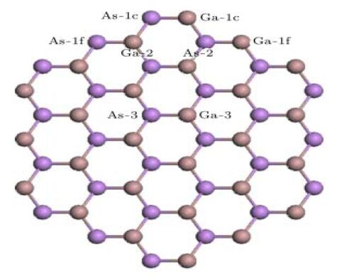
Top view of the ideal atomic structures for Te-Ga and Te-As GaAs NWs (The different substitutional Ga and As sites with a single Te atom are labeled and numbered. The rust red and bluish violet balls donate Ga and As atoms, respectively)
Figure 1.
Top view of the ideal atomic structures for Te-Ga and Te-As GaAs NWs (The different substitutional Ga and As sites with a single Te atom are labeled and numbered. The rust red and bluish violet balls donate Ga and As atoms, respectively)
Citation:
LAN Zi-Ping, WEI Xiang-Hai, WANG Hai-Feng, LI Quan, GAO Tao. Structural, Electronic and Optical Properties of Te-Doped GaAs Nanowires: the First Principles Study①[J]. Chinese Journal of Structural Chemistry,
2016, 35(7): 993-1001.
doi:
10.14102/j.cnki.0254-5861.2011-1062

Structural, Electronic and Optical Properties of Te-Doped GaAs Nanowires: the First Principles Study①
English
Structural, Electronic and Optical Properties of Te-Doped GaAs Nanowires: the First Principles Study①
Abstract:
The first-principles calculations have been performed to determine the effects of Te doping to the structural, electronic, and optical properties of GaAs NWs. The calculated formation energies show that the single Te energetically prefers to substitute the core Ga (Ef=0.4111 eV) under As-rich conditions of GaAs nanowires, while on surface, the single Te tends to substitute the surface As site. With increasing the Te concentration, the favorable substitution sites are 2Te-Ga-A and 3Te-Ga-D. Thus, the stability of the structure of the electronic structure and optical properties are discussed.
-
Key words:
- GaAs nanowires
- / electronic structure
- / optical properties
- / density functional theory
-
1 INTRODUCTION
Owing to the unique properties arising due to their nanoscale radial footprints[1], III−V semiconductor nanowires (NWs) continue to generate intense interest[2, 3]. NW-based electronic and photonic devices such as solar cells, lasers, light-emitting diodes, photodetectors, and transistors have already been demonstrated[4-6]. Among binary III−V semiconductors, GaAs with a direct bandgap of 1.42 eV and with very high electron mobility (~8500 cm2⋅V−1⋅s−1) is particularly promising for photovoltaic and high-frequency applications[7, 8]. However, GaAs also has the highest known surface recombination rate (~106 cm⋅s−1) of charge carriers among III−V materials. Further, GaAs NWs, in particular, are associated with a very high density of surface states that promote undesirable nonradiative recombination channels at the NW surface[9].
Similar to bulk crystals, researchers have envisioned GaAs nanowires to be a potential alternative for Si nanowires[10]. Recent advances in fabrication technology made it possible to grow GaAs nanowires. They are grown by metal catalysts in vapor-liquid-solid [VLS] mechanism[11]. Generally, GaAs nanowires are grown along the [111] direction in zinc-blende(zb) structure, whereas nanowires with wurtzite structure with diameter as small as 10 nm are also observed[12, 13]. Several models are developed to predict the transition radius from wurtzite to zinc-blende structures. Actually, there is no sharp transition but instead there are many different stacking configurations with very similar energies and more sophisticated models are needed to predict the ground-state configuration. Together with the crystal structure, surface facet structure is also an important parameter affecting the structural and electronic properties[14].
Unfortunately, pure semiconductor NWs have low concentration of carries due to the increasing band gap with the decrease of NW size[15, 16]. It is now commonly accepted that doping is an essential way to provide free carries. Many theoretical models have been proposed to examine the properties of dopants incorporation[17, 18]. Also a first-principles investigation has been addressed on the Mn-doped III-V NWs, which was concentrated on the electronic and magnetic properties of (Ga, Mn)As and (In, Mn)As NWs[19-21].
In this article, the stability of various doping sites by comparing their formation energies is investigated, and the detailed electronic structures are computed. It is expected that our work can provide some valuable information on the synthesis of Te-doped GaAs NW materials with specific applications.
2 COMPUTATIONAL METHODS
In this study, the first-principles band-structure calculations are performed with the local density approximation (LDA) based density functional theory (DFT)[18, 21], as implemented in the Vienna ab initio simulation package (VASP)[22]. The projected augmented wave (PAW) method is chosen to represent the ionic potentials. The Monkhorst-Pack method is used to sample the Brillouin zone. For all nanowires, a 1 × 1 × 9 k-grid is used. For all calculations, the energy cut off for the plane waves is 300 eV. The convergency with respect to the plane wave basis cutoff energy and the k-sampling is checked to be within 10-5 eV. Before the electronic structure properties were studied, the atomic configurations for all structures have been relaxed until the Hellmann-Feynman force is less than 0.01 eV⋅Å−1.
The interaction of a photon with the electrons can be described in terms of time-dependent perturbations of the ground state electronic states. The electric field of the photon leads to the transition between occupied and unoccupied states, including plasmons and single-particle excitations. The excitation spectra can be described as a joint density of states between the valence and conduction bands. The optical properties are determined by the dielectric function ε(ω) =ε1(ω) + iε2(ω), which is mainly contributed from the electronic structures. The imaginary part ε2(ω) of dielectric function could be obtained from the momentum matrix elements between the occupied and unoccupied wave functions, and the real part ε1(ω) can be evaluated from ε2(ω) using the Kramer-Kronig relations[23]:
Arising from ε1(ω) and ε2(ω), all of the other optical properties, such as reflectivity
R(ω) and absorption coefficient α(ω), can be calculated:
3 RESULTS AND DISCUSSION
3.1 Model structures and relative stability of Te-doped GaAs NW
The structural properties of defect-free GaAs NWs prior to studying the defects are first investigated. For a single Te (1.85% Ag-doping concentration) incorporation, our results show that the structures are high-energy configurations for interstitial dopants. In other words, these configurations are difficult to form. Therefore, two kinds of doping configurations are considered, including one substitutional Ag at Ga (Te-Ga) and one substitutional Ag at the As site (Te-As). The specific substitutional sites have been plotted in Fig. 1, which indicates that four different Ga sites can be replaced by Te, labeled as Te-1c, Te-1f, Te-2 and Te-3, respectively. The replacement of the As atom with Te is the same as Ga.
Figure 1.
Top view of the ideal atomic structures for Te-Ga and Te-As GaAs NWs (The different substitutional Ga and As sites with a single Te atom are labeled and numbered. The rust red and bluish violet balls donate Ga and As atoms, respectively)
The formation energy of these impurities in the charge neutral state is defined by[24]:
Ef = E(Te:GaAs)-E(GaAs) + ΔnGaμGa + ΔnAsμAs-ΔnTeμTe
where E(Te:GaAs) and E(GaAs) are the total energies of the supercell with and without impurities, respectively; Δn is the number of ions (Ga, As or Te) changed between a pristine supercell and its corresponding reservoir to form a defect; and μ is the chemical potential of Ga, As or Te. Here, two chemical potential extremes are considered. The upper limits for μGa(Ga-rich) and μAs(As-rich) are decided as the total energies of the metallic Ga and simple substance (ss) per atom, respectively. The lower levels are obtained from the thermodynamic equilibrium:
μGa+μAs = μGaAsNW
where μGaAsNW is defined as the total energies of GaAs NWs per Ga−As atom pair.
Therefore,
μGa(As-rich) = μGa(metal) + ΔHf(GaAsNW)
and
μAs(Ga-rich) = μAs(ss) + ΔHf(GaAsNW)
where the heat of formation of GaAsNW
ΔHf(GaAsNW) = μGaAsNW −μGa(metal)-μAs(ss)
Additionally, the reservoir chosen for Ag is GaTe, and the chemical potential of Te under the two limiting Ga conditions is obtained from the thermodynamic equilibrium: μGa + μTe = μGaTe
Table 1 gives the computed formation energies for individual Te dopants in different sites, and shows that Te incorporation prefers to occupy the Ga site (Ef = 0.4111 eV). It is interesting that the Te replacements of the surface Ga atom (Te-1c) are equivalent in energy for both the Ga- and As-rich conditions. However, the surface As (Te-1f) (0.1947 eV) site becomes more competitive in energy compared with As (Te-1c) (0.3963 eV) under Ga-rich conditions.
 Table 1.
Formation Energies Ef (eV) of Single Te Substitutions in the GaAs NWs under Both G a-rich and As-rich Conditions
Table 1.
Formation Energies Ef (eV) of Single Te Substitutions in the GaAs NWs under Both G a-rich and As-rich Conditions
Ef (eV) Defects Te-Ga Positions Te-1c Ga-rich 0.4309 As-rich 0.4111 Te-1f 0.5828 0.5629 Te-2 1.4774 1.4615 Te-3 1.9859 1.9661 Te-As Te-1c 0.3963 0.4163 Te-1f 0.1947 0.2147 Te-2 0.7771 0.7971 Te-3 0.8579 0.8779 Table 1. Formation Energies Ef (eV) of Single Te Substitutions in the GaAs NWs under Both G a-rich and As-rich ConditionsDoping with a higher concentration of 3.70% has also been modeled by incorporating a pair of Ga atoms with two Ag atoms in the NW supercell. In light of these arguments that Te-Ga substitution in the surface is more stable than that in the core of NW, it is proposed that possible double Te replacements occur at the surface and subsurface layers of the NW models, as shown in Fig. 2. Specifically, the A, B, and C configurations correspond to Te incorporations of the nearest-neighbor Gas-Gas, Gas-Gasub and Gas-Gac in the same (10-10) layer; configurations D and E correspond to Te incorporations of the nearest-neighbor Gas-Gas and Gas-Gasub in different (10-10) layers; and configuration F corresponds to Te incorporation of the second-nearest-neighbor Gas-Gas in the same (10-10) layer.
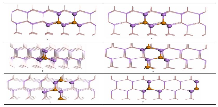 Figure 2.
Side views of six configurations for the 2Te-Ga substitutions in the GaAs NW, named A, B, C, D, E and F
Figure 2.
Side views of six configurations for the 2Te-Ga substitutions in the GaAs NW, named A, B, C, D, E and F
The calculated formation energies in Table 2 show that all of the 2Te-Ga configurations are easier to form under the As-rich conditions. Surprisingly, to some extent, configuration A (0.3159 eV) is favorable in energy under As-rich conditions. In light of these arguments, the double Te defects prefer to occupy the nearest-neighbor Gas-Gas, as suggested by this study.
Table 2.
Formation Energies Ef (eV) of Double Te Substitutions in the GaAs NWs under Both Ga-rich and As-rich Conditions
Ef(eV) Defects 2Te-Ga Positions A Ga-rich 0.3557 As-rich 0.3159 B 1.7055 1.6658 C 2.3603 2.3206 D 0.7329 0.6933 E 1.1669 1.1273 F 0.8550 0.8154 Table 2. Formation Energies Ef (eV) of Double Te Substitutions in the GaAs NWs under Both Ga-rich and As-rich ConditionsMore interestingly, a higher dopant concentration of 5.56% has been examined by substituting three Ga atoms with three Te atoms in the 108 (Ga54As54) atom GaAs NW supercell. As shown in Fig. 3, six different structures are proposed: configurations A, B, C and D correspond to the Te replacement of 3Gas, 2Gas-Gasub, 2Gas-Gac and Gas-Gasub-Gac in the same (10-10) layer; and configurations E and F correspond to the Ag substitution of 2Gas-Gasub and 2Gas-Gac in different (10-10) layers. The formation energies of 3Te-Ga are listed in Table 3.
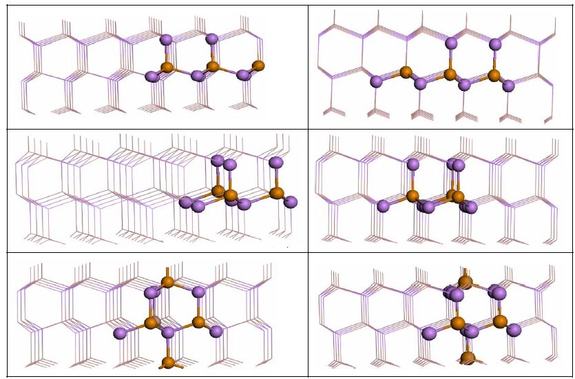 Figure 3.
Side views of six configurations for 3Te-Ga substitutions in GaAs NW, named A, B, C, D, E and F
Table 3.
Formation Energies Ef (eV) of 3Te-Ga
Figure 3.
Side views of six configurations for 3Te-Ga substitutions in GaAs NW, named A, B, C, D, E and F
Table 3.
Formation Energies Ef (eV) of 3Te-Ga
Ef(eV) Defects Positions Ga-rich As-rich 3Te-Ga A 0.7852 0.6457 B 1.7510 1.6113 C 2.2064 2.0669 D 0.3487 0.2095 E 1.2512 1.1117 F 2.2958 2.2063 Table 3. Formation Energies Ef (eV) of 3Te-GaThe formation energies of 3Te-Ga are listed in Table 3. It can be found that the three substitution-Te atoms at the 3Gas sites (3Te-Ga-D) are the most energetically favorable configurations, and that the calculated formation energy for the 3Te-Ga-D model is 0.2095 eV under As-rich conditions. In light of these arguments, the 3Te defects prefer to occupy the Ga sites in different (10-10) layers.
3.2 Electronic structures of Te-doped GaAs NW
To investigate the influence of Te dopants on the modification of electronic structures, the calculated band structures of Te-Ga and Te-As dopant configurations on bare GaAs NWs are shown in Fig. 4 for comparison of stability. From Fig. 4, it can be seen that both the CBM (minimum of conduction band) and VBM (maximum of valence band) are located at the Γ point in the Brillouin zone. The results indicate that the GaAs NWs are a direct band gap semiconductor.
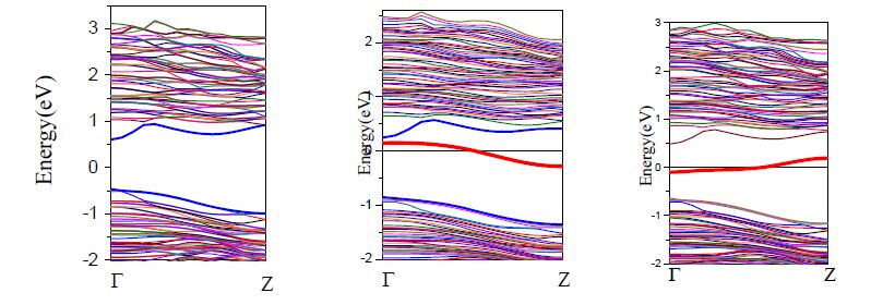 Figure 4.
Band structures of undope and Te-dope (Te-Ga and Te-As)
Figure 4.
Band structures of undope and Te-dope (Te-Ga and Te-As)
If not introducing the tellurium band at first, we can not determine the type of semiconductor from band structure, i.e., direct or indirect gap semiconductor; while with the dopant of element tellurium, the semiconductor of direct band gap is indicated in Fig. 4, no matter which atom, gallium and arsenic, in GaAs NW is substituted, and this substitution does not lead obvious change of the band gap for GaAs NW, with their values to be 1.08, 1.11 and 1.11 eV, respectively.
However, it can be seen that the impurity state conduction band and valence band drop obviously after element doped from the Fig. 4. For example, on one hand, when single tellurium replaces a gallium atom (Te-Ga) in GaAs NW, the maximum of valence band drops from -0.47 to -0.85 eV, the minimum of conduction band drops 0.59 eV to 0.47 eV. On the other hand, when a single arsenic replaced by a tellurium in GaAs NW (Te-As), the maximum of valence band decreases from the original -0.47 to -0.63 eV, and the decreased value for conduction band is about 0.33 eV. These data are hopefully used to the fabrication of corresponding GaAs NW.
As can be seen from Fig. 4, a gallium replaced by a tellurium (Te-Ga) on top of the valence band of 0.98 eV will produce an impurity band. In a similar way, when an arsenic atom is replaced by a tellurium (Te-As), an impurity band is also produced on the top of valence band of -0.73 eV. Both of them belong to the heavily-doped type. In addition, we can see that the doping can change the semiconductor behavior of nanowires. For example, if a gallium atom is replaced by a tellurium, the type of the band gap will change from direct to indirect semiconductor. However, if an arsenic atom is replaced by a tellurium, the type of the band gap will not change, i.e., still direct band gap.
We have also investigated the behavior of two tellurium atoms doping, which are displayed in Fig. 5. The two gallium atoms are replaced by tellurium atoms which are two nearest neighboring positions. The impurity bands of the two tellurium atoms are located at 0.80 and -0.45 eV in the band structures, respectively. There is a very big energy difference between the top of the valence band and the bottom of conduction band which are coming from the impurities. It indicates that two atoms doping is heavier than that of the single tellurium doping, and also of a P-type doping. We can observe that one band on the top of valence shifts up compared with that before doping, which makes the energy band gap decrease. In addition, the type of band gap is changed from direct to indirect semiconductor when tellurium doping.
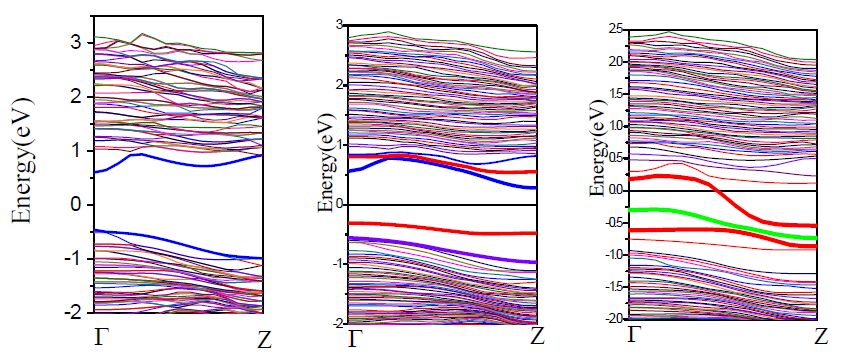 Figure 5.
Band structures of undoped and Te-doped (Te-Ga and Te-As)
Figure 5.
Band structures of undoped and Te-doped (Te-Ga and Te-As)
Finally, we studied the behavior of three tellurium atoms doping. When three tellurium atoms are introduced, the first valence band and the conduction band did not have much shift. The effect is that the space of the band structure is broaden, and the three impurity states are located at the top of the valance band with the values of 0.14, -0.44 and -0.59, respectively. Compared with single doping, it is of lighter-doped type. We can seen that one band level of the three impurity states is across the Fermi level, and the other two band levels are below in the Fermi level, indicating that it is a typical N-type doping and the type of band gap is changed when three tellurium doping. In summary, the behavior of gallium atoms replaced by tellurium atoms belongs to N-type doping, which is independent of the concentration of the doping element.
3.3 Optical properties of Te-doped GaAs NW
In this section, the optical properties of absorption spectrum of Te-doped GaAs NW are systematically discussed. The results are shown in Fig. 6 and compared with the pure nanowires. Optical absorption spectrum of all combination is shown in Fig. 6. The doping of Ga and As atoms by single Te atom shifts red. And the shift value of Te replacing Ga is greater than that of As in nanowire duo to the Te is non-metallic. The properties are changed little when Te replaces As. With the increase of concentration of Te impurity, the red shift value is also increased, which indicates a significant quantum confinement effect. With increasing the concentration of doped tellurium, the absorption spectrum gets stable compared with the pure nanowires because the position of Ga atoms in GaAs nanowires is of metallic properties before doping. With the increase of doping concentration, the absorption edge shifts red gradually.
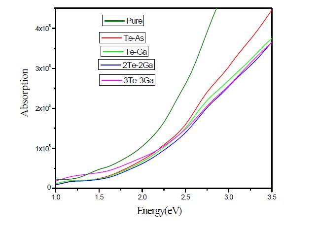 Figure 6.
Absorption coefficient spectra of Te-doped GaAs NW as compared with those of pure NW
Figure 6.
Absorption coefficient spectra of Te-doped GaAs NW as compared with those of pure NW
From the above analysis, we can find that the element doping plays an important role in the optical transition process. Compared with the different concentrations of doping, we can find that the inhibition effect gets stronger with the increase of doping concentration in the WZ-3 gallium arsenide nanowires system.
4 CONCLUSION
In summary, the first-principles calculations have been performed to study the geometric, electronic, and optical properties of different defects in Tedoped GaAs NW.
(a) The results show that the properties of nanowire with elements doping will be changed, e.g., if the gallium atom is replaced by a tellurium, the type of the band gap will change from direct to indirect. However, if an arsenic atom is replaced by a tellurium, the type of the band gap will not change, and they show direct band gaps. The two gallium atoms are replaced by tellurium atoms which are two nearest neighboring positions. The impurity bands of the two tellurium atoms are located at 0.80 and -0.45 eV in the band structures, respectively. We can observe that one band on the top of valence shifts up compared with that before doping, which makes the energy band gap decrease. In addition, the type of band gap is changed from direct to indirect semiconductor with tellurium doping. When three tellurium atoms are introduced, the first valence band and the conduction band did not have much shift. The effect is that the space of the band structure is broadened. The three impurity states are located at the top of the valance band with the values of 0.14, -0.44 and -0.59, respectively.
(b) The elements doping plays an important role in the optical transition process. Compared with the different concentrations of doping, the inhibition effect gets stronger with the increase of doping concentration in the WZ-3 gallium arsenide nanowires system.
The physical properties of nanomaterials have become one of the hottest researches in condensed matter physics. The one-dimensional semiconductor nanowires and nanotubes have received much attention because of their unique properties and more popular applications. The systematic study of GaAs nanowires in this paper will provide useful reference to other related physical properties in nanowires researches.
-
-
[1]
Lü X., Shen W. Z., Chu J. H.. Size effect on the thermal conductivity of nanowires[J]. J. App. Phys., 2002, 3: 1542-1552.
-
[2]
Tereshchenko O. E., Bakulin A. V., Kulkova S. E., Eremeev S. V.. Backward reconstructions on GaAs(001) surface induced by atomic hydrogen reactions: surfactant-assisted low-temperature surface ordering[J]. J. Phys. Chem. C, 2013, 19: 9723-9733.
-
[3]
Glas, F.; Harmand, J. C.; Patriarche, G. Why does wurtzite form in nanowires of III-V zinc blende semiconductors? Phys. Rev. Lett. 2007, 14, 1−4.
-
[4]
Agrawal R., Espinosa H. D.. Giant piezoelectric size effects in zinc oxide and gallium nitride nanowires[J]. A first principles investigation. Nano. Lett., 2011, 2: 786-790.
-
[5]
Ahtapodov L., Todorovic J., Olk P., Mjåland T., Sl?ttnes P., Dheeraj D. L; Weman, H.. A story told by a single nanowire: optical properties of wurtzite GaAs[J]. Nano. Lett., 2012, 12: 6090-6095. doi: 10.1021/nl3025714
-
[6]
Du Y. A., Sakong S., Kratzer P.. As vacancies, Ga antisites, and Au impurities in zinc blende and wurtzite GaAs nanowire segments from first principles[J]. Phys. Rev. B, 2013, 7: 075308.
-
[7]
Estrin Y., Rich D. H., Kretinin A. V., Shtrikman H.. Influence of metal deposition on exciton-surface plasmon polariton coupling in GaAs/AlAs/GaAs core-shell nanowires studied with time-resolved cathodoluminescence[J]. Nano. Lett., 2013, 4: 1602-1610.
-
[8]
Cahangirov S., Ciraci S.. First-principles study of GaAs nanowires[J]. Phys. Rev. B, 2009, 16: 165118.
-
[9]
Dufouleur J., Colombo C., Garma T., Ketterer B., Uccelli E., Nicotra M., Fontcuberta I., Morral A.. P-doping mechanisms in catalyst-free gallium arsenide nanowires[J]. Nano. Lett., 2010, 5: 1734-1740.
-
[10]
Chen H., Shi D., Qi J., Jia J., Wang B.. The stability and electronic properties of wurtzite and zinc-blende ZnS nanowires[J]. Phys. Lett. A, 2009, 3: 371-375.
-
[11]
Heiss M., Conesa-Boj S., Ren J., Tseng H. H., Gali A., Rudolph A., Reiger E.. Direct correlation of crystal structure and optical properties in wurtzite/zinc-blende GaAs nanowire heterostructures[J]. Phys. Rev. B, 2011, 4: 1-10.
-
[12]
Raghunathan R., Johlin E., Grossman J. C.. Grain boundary engineering for improved thin silicon photovoltaics[J]. Nano. Lett., 2014, 9: 4943-4950.
-
[13]
Harb M., Sautet P., Raybaud P.. Anionic or cationic S-doping in bulk anatase TiO2: insights on optical bbsorption from first principles calculations[J]. J. Phys. Chem. C, 2013, 17: 8892-8902.
-
[14]
Dhaka V., Oksanen J., Jiang H., Haggren T., Nykänen A., Sanatinia R., Anand S.. Aluminum-induced photoluminescence red shifts in core-shell GaAs/Al x Ga1–x As nanowires[J]. Nano. Lett., 2013, 13: 3581-3588. doi: 10.1021/nl4012613
-
[15]
Galicka M., Buczko R., Kacman P.. Structure-dependent ferromagnetism in Mn-doped IIIV nanowires[J]. Nano. Lett., 2011, 8: 3319-3323.
-
[16]
Ghaderi N., Peressi M., Binggeli N., Akbarzadeh H.. Structural properties and energetics of intrinsic and Si-doped GaAs nanowires: first-principles pseudopotential calculations[J]. Phys. Rev. B, 2010, 15: 1-9.
-
[17]
Li Y., Zhao X., Fan W.. Structural, electronic, and optical properties of Ag-doped ZnO nanowires: first principles study[J]. J. Phys. Chem. C, 2011, 9: 3552-3557.
-
[18]
Kresse G., Hafner J.. Ab Initio molecular-dynamics simulation of the liquid-metal-amorphous-semiconductor transition in germanium[J]. Phys. Rev. B, 1994, 20: 14251-14269.
-
[19]
Li Y., Zhao X., Fan W., Sun H., Cheng X.. Role of cross section on the stability and electronic structure of Ag-doped ZnO nanowires[J]. J. Nanoparticle Res., 2012, 3: 1-10.
-
[20]
Ihn S. G., Ryu M. Y., Song J. I.. Optical properties of undoped, Be-doped, and Si-doped wurtzite-rich GaAs nanowires grown on Si substrates by molecular beam epitaxy[J]. Solid State Commun., 2010, 15: 729-733.
-
[21]
Kresse G., Furthmüller J.. Efficiency of ab-initio total energy calculations for metals and semiconductors using a plane-wave basis set[J]. Comp. Mater. Sci., 1996, 1: 15-50.
-
[22]
Kresse G., Joubert D.. From ultrasoft pseudopotentials to the projector augmented-wave method[J]. Phys. Rev. B, 1999, 3: 1758-1775.
-
[23]
Shi H., Chu M., Zhang P.. Optical properties of UO2 and PuO2. J. Nucl[J]. Mater., 2010, 2: 151-156.
-
[24]
Lei W., Tao G., Ma S. J., Lu P. F., Peng L.. First-principles study of Ag-doped GaAs nanowires[J]. Chin. Phys. Lett., 2013, 6: 1-5.
-
[1]
-

Figure 1 Top view of the ideal atomic structures for Te-Ga and Te-As GaAs NWs (The different substitutional Ga and As sites with a single Te atom are labeled and numbered. The rust red and bluish violet balls donate Ga and As atoms, respectively)

Figure 2 Side views of six configurations for the 2Te-Ga substitutions in the GaAs NW, named A, B, C, D, E and F

Figure 3 Side views of six configurations for 3Te-Ga substitutions in GaAs NW, named A, B, C, D, E and F

Figure 6 Absorption coefficient spectra of Te-doped GaAs NW as compared with those of pure NW
Table 1. Formation Energies Ef (eV) of Single Te Substitutions in the GaAs NWs under Both G a-rich and As-rich Conditions
Ef (eV) Defects Te-Ga Positions Te-1c Ga-rich 0.4309 As-rich 0.4111 Te-1f 0.5828 0.5629 Te-2 1.4774 1.4615 Te-3 1.9859 1.9661 Te-As Te-1c 0.3963 0.4163 Te-1f 0.1947 0.2147 Te-2 0.7771 0.7971 Te-3 0.8579 0.8779  下载: 导出CSV
Table 2. Formation Energies Ef (eV) of Double Te Substitutions in the GaAs NWs under Both Ga-rich and As-rich Conditions
Ef(eV) Defects 2Te-Ga Positions A Ga-rich 0.3557 As-rich 0.3159 B 1.7055 1.6658 C 2.3603 2.3206 D 0.7329 0.6933 E 1.1669 1.1273 F 0.8550 0.8154
下载: 导出CSV
Table 3. Formation Energies Ef (eV) of 3Te-Ga
Ef(eV) Defects Positions Ga-rich As-rich 3Te-Ga A 0.7852 0.6457 B 1.7510 1.6113 C 2.2064 2.0669 D 0.3487 0.2095 E 1.2512 1.1117 F 2.2958 2.2063
下载: 导出CSV
-


 扫一扫看文章
计量
- PDF下载量: 21
- 文章访问数: 1849
- HTML全文浏览量: 283
 下载:
下载:
