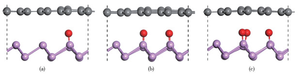
Figure 1.
Side views of $\mathrm{BP} / \mathrm{Gr}$ $\mathrm{O}$
Schottky barrier of blue phosphorus/graphene heterostructure regulated by the adsorption of oxygen atoms
Wang-Yang DUAN , Yue-Huan CHENG , Ji-Song HU , Xin-Guo MA , Ling PEI

Phosphene has attracted attention due to its extremely high carrier mobility. It has an excellent performance in the fields of electrocatalysis [1], photovoltaic power generation [2], energy storage [3] and transistors [4]. Besides, it is a strong candidate for the next generation of nano-electronic devices. There are theoretically 9 forms of phosphorene monolayer, including
In a device with phosphorene as the channel, a Schottky barrier is often formed at the interface of metal electrodes and phosphorene, which would reduce the carrier injection efficiency [10]. In order to explain and address these issues, for example, five representative metal systems such as
As experiments and theories improve by leaps and bounds, much research has been carried out to solve this problem. What is known to us is that twodimensional (2D) materials enjoy numerous exceptional advantages over conventional materials on a quantum scale, for instance, graphene has lower losses and higher carrier mobility [18]. Recently, it was accounted for that a heterostructure can be changed from a n-type Schottky contact to a p-type Schottky contact with increasing of compressive strain [19]. Afterwards, Li et al. [13] affirmed that the electric field was compelling to tune the Schottky barrier for the BP/Gr interface, which can change the n-type into the p-type. Thus, graphene can be used as a low-resistance contact material to replace noble metals. And it is noteworthy that, Liang et al. reported a high - performance anisotropic graphene/black phosphorus heterostructure with promising potential applications in electronic devices [20-22]. These achievements provide ideas for us to tune the Schottky barrier of the BP/Gr heterostructures by O - doped. In this work, first-principles calculations on the
All calculations were performed using Ultrasoft Pseudopotentials (USP) and using the Generalized Gradient Approximation (GGA)-Perdew Burke Ernzerhof (PBE) [23] form based on the CASTEP [24] implementation of the Generalized Gradient Approximation in Density Functional Theory (DFT) exchange and association. In the USP calculations, a mixed semi-empirical solution of the Grimme [25] and Ortmann - Bechstedt Schmidt (OBS) [26] schemes is provided to introduce the correct description of van der Waals (vdW) interactions. The dispersion-corrected total energy
Before exploring the performance of the
 下载:
导出CSV
下载:
导出CSV
| Heterojunction | Energy |
|||||||||||
| Mismatch | Cohesive | |||||||||||
| 0.327 | 0.327 | 0.247 | 0.247 | 0.98 | 0.98 | 0.714 | 0.714 | 0.3 | -1.4 | |||
| 0.327 | 0.327 | 0.247 | 0.247 | 0.983 | 0.984 | 0.714 | 0.714 | 2 | -5.8 | |||
| 0.327 | 0.327 | 0.247 | 0.247 | 0.984 | 0.983 | 0.714 | 0.714 | 2.4 | -9.2 | |||
| 0.327 | 0.327 | 0.248 | 0.248 | 0.983 | 0.985 | 1.121 | 1.121 | 11.9 | -10.6 | |||
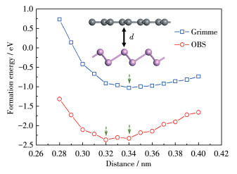
The interfacial formation energies of heterojunctions at different interlayer distances
|
|
(1) |
where
The interlayer interactions of a heterostructure have a huge impact on electronic structure. In order to obtain a stable geometrical structure of
|
|
(2) |
where
The lattice mismatch energy of the BP/Gr heterojunction under strain can be estimated as:
|
|
(3) |
where
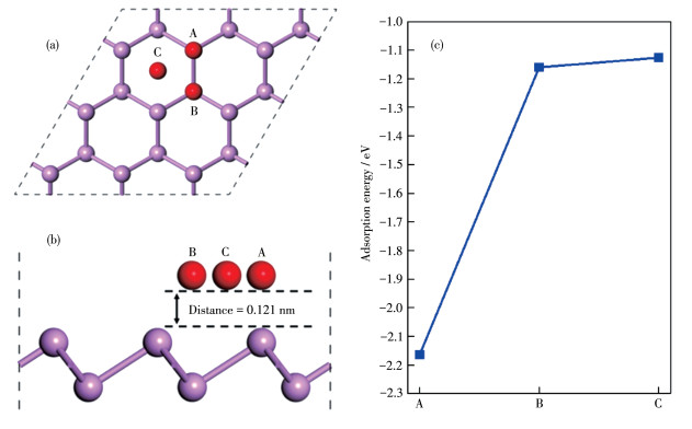
On the surface of the BP monolayer, three types of high symmetry adsorption sites exist: (ⅰ) A sites over a
To understand the
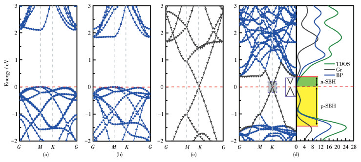
The n-type (p-type) SBH are indicated between the Femi level and the conduction band minimum (the valence band maximum) of the BP monolayer; the Fermi level is set to zero and marked by red dotted lines.
It can be seen that due to the large equilibrium interlayer distance
To realize more efficient logic devices based on phosphorene, it is necessary to fabricate
As the concentration of
A Schottky barrier is formed at this interface between graphene and BP monolayer. The SBH of the
In order to investigate the effect of
|
|
(4) |
where
The blue and red dashed lines denote the vacuum energy level and Fermi level, respectively.
To understand how the Fermi level of the BP/Gr heterostructures varies with the concentration of
The formation of heterostructures can alter the electrical properties of heterostructures and BP monolayer or graphene, due to interlayer interactions and interfacial charge redistribution. Therefore, we calculated the three-dimensional (3D) charge density difference, revealing the interlayer charge transfer and separation between the
The isovalue chosen to plot the isosurface is
In order to quantitatively analyze the redistribution of interfacial charges at the interface, the planar averaged charge density differences along the
The results of Mulliken population analysis show that the charge transfer and redistribution inside and outside the interface varies with
In summary, the microscopic mechanisms of interface interactions by
Chen H, Chen J, Ning P, Chen X, Liang J, Yao X, Chen D, Qin L, Huang Y, Wen Z. 2D heterostructure of amorphous cofeb coating black phosphorus nanosheets with optimal oxygen intermediate absorption for improved electrocatalytic water oxidation[J]. ACS Nano, 2021, 15(7): 12418-12428. doi: 10.1021/acsnano.1c04715
Zhang M, Ye M, Wang W, Ma C, Wang S, Liu Q, Lian T, Huang J, Lin Z. Synergistic cascade carrier extraction via dual interfacial positioning of ambipolar black phosphorene for high- efficiency perovskite solar Cells[J]. Adv. Mater., 2020, 32(28): e2000999. doi: 10.1002/adma.202000999
Tao Y P, Huang T, Ding C X, Feng Y, Tan D M, Wang F X, Xie Q J, Yao S Z. Few-layer phosphorene: An emerging electrode material for electrochemical energy storage[J]. Appl. Mater. Today, 2019, 15: 18-33. doi: 10.1016/j.apmt.2018.12.008
Fang R H, Cui X Y, Khan M A, Stampfl C, Ringer S P, Zheng R K. Strain-engineered ultrahigh mobility in phosphorene for terahertz transistors[J]. Adv. Electron. Mater., 2019, 5(3): 1800797. doi: 10.1002/aelm.201800797
Wu M, Fu H, Zhou L, Yao K, Zeng X C. Nine new phosphorene polymorphs with non- honeycomb structures: a much extended family[J]. Nano Lett., 2015, 15(5): 3557-3562. doi: 10.1021/acs.nanolett.5b01041
He C, Zhang C, Tang C, Ouyang T, Li J, Zhong J. Five low energy phosphorene allotropes constructed through gene segments recombination[J]. Sci. Rep., 2017, 7: 46431. doi: 10.1038/srep46431
Zhang L, Huang H, Zhang B, Gu M, Zhao D, Zhao X, Li L, Zhou J, Wu K, Cheng Y, Zhang J. Structure and properties of violet phosphorus and its phosphorene exfoliation[J]. Angew. Chem. Int. Ed., 2020, 59(3): 1074-1080. doi: 10.1002/anie.201912761
Zhu Z, Tomanek D. Semiconducting layered blue phosphorus: a computational study[J]. Phys. Rev. Lett., 2014, 112(17): 176802. doi: 10.1103/PhysRevLett.112.176802
Xiao J, Long M, Zhang X, Ouyang J, Xu H, Gao Y. Theoretical predictions on the electronic structure and charge carrier mobility in 2D phosphorus sheets[J]. Sci. Rep., 2015, 5: 9961. doi: 10.1038/srep09961
Li J Z, Sun X T, Xu C Y, Zhang X Y, Pan Y Y, Ye M, Song Z G, Quhe R G, W Y Y, Zhang H, Guo Y, Yang J B, Pan F, Lu J. Electrical contacts in monolayer blue phosphorene devices[J]. Nano Res., 2018, 11(4): 1834-1849. doi: 10.1007/s12274-017-1801-2
Montes E, Schwingenschlögl U. High-Performance Field-Effect Transistors Based on alphaP and betaP[J]. Adv. Mater., 2019, 31(18): e1807810. doi: 10.1002/adma.201807810
Zhu S C, Hu T Y, Yip C T, Yao K L, Lam C H. Interface effect between blue phosphorus and metals[J]. Phys. Lett. A, 2020, 384(23): 126554. doi: 10.1016/j.physleta.2020.126554
Li H L, Cui Y T, Luo H J, Wang T, Li D M. Tuneable Schottky barrier in van der Waals graphene-blue phosphorus heterojunction[J]. Physica B Condens. Matter, 2019, 560: 75-80. doi: 10.1016/j.physb.2019.02.027
Musso T, Kumar P V, Foster A S, Grossman J C. Graphene oxide as a promising hole injection layer for MoS2- based electronic devices[J]. ACS Nano, 2014, 8(11): 11432-11439. doi: 10.1021/nn504507u
Tung R T. Chemical bonding and fermi level pinning at metal-semiconductor interfaces[J]. Phys. Rev. Lett., 2000, 84: 6078-6081. doi: 10.1103/PhysRevLett.84.6078
Tung R T. The physics and chemistry of the Schottky barrier height[J]. Appl. Phys. Rev., 2014, 1(1): 011304. doi: 10.1063/1.4858400
Liu Y, Guo J, Zhu E, Liao L, Lee S J, Ding M, Shakir I, Gambin V, Huang Y, Duan X. Approaching the schottky- mott limit in van der waals metal-semiconductor junctions[J]. Nature, 2018, 557(7707): 696-700. doi: 10.1038/s41586-018-0129-8
Loh K P, Bao Q L, Ang P K, Yang J X. The chemistry of graphene[J]. J. Mater. Chem., 2010, 20(12): 2277. doi: 10.1039/b920539j
Zhu J D, Zhang J C, Hao Y. Tunable schottky barrier in blue phosphorus- graphene heterojunction with normal strain[J]. Jpn. J. Appl. Phys., 2016, 55(8): 080306. doi: 10.7567/JJAP.55.080306
Liang J M, Lei J T, Wang Y, Ding Y, Shen Y, Deng X H. High performance terahertz anisotropic absorption in graphene- black phos- phorus heterostructure*[J]. Chin. Phys. B, 2020, 29(8): 087805. doi: 10.1088/1674-1056/ab9cbf
广东工业大学. 一种电致图案化黑磷烯/石墨烯电极的制备方法: CN202111004595.4. 2021-11-30.Guangdong University of Technology. Preparation method of electropatterned black phosphorene/graphene electrode and apparatus thereof: CN202111004595.4. 2021-11-30.
Li S T, Zhang Y H, Huang H W. Black phosphorus- based hetero- structures for photocatalysis and photoelectrochemical water splitting[J]. J. Energy Chem., 2022, 67: 745-779. doi: 10.1016/j.jechem.2021.11.023
Perdew J P, Burke K, Ernzerhof M. Generalized gradient approximation made simple[J]. Phys. Rev. Lett., 1996, 77(18): 3865-3868. doi: 10.1103/PhysRevLett.77.3865
Ceperley D M, Alder B J. Ground state of the electron gas by a stochastic method[J]. Phys. Rev. Lett., 1980, 45(7): 566-569. doi: 10.1103/PhysRevLett.45.566
Grimme S. Semiempirical GGA-type density functional constructed with a long-range dispersion correction[J]. J. Comput. Chem., 2006, 27(15): 1787-1799. doi: 10.1002/jcc.20495
Ortmann F, Bechstedt F, Schmidt W G. Semiempirical van der Waals correction to the density functional description of solids and molecular structures[J]. Phys. Rev. B, 2006, 73(20): 205101. doi: 10.1103/PhysRevB.73.205101
Ma X, Wei Y, Wei Z, He H, Huang C, Zhu Y. Probing π-π stacking modulation of g-C3N4/graphene heterojunctions and corresponding role of graphene on photocatalytic activity[J]. J. Colloid Interface Sci., 2017, 508: 274-281. doi: 10.1016/j.jcis.2017.08.037
Monkhorst H J, Pack J D. Special points for Brillouin-zone integrations[J]. Phys. Rev. B, 1976, 13(12): 5188-5192. doi: 10.1103/PhysRevB.13.5188
Zhang J L, Zhao S, Han C, Wang Z Z, Zhong S, Sun S, Guo R, Zhou X, Gu C D, Yuan K D, Li Z Y, Chen W. Epitaxial growth of single layer blue phosphorus: A new phase of two-dimensional phosphorus[J]. Nano Lett., 2016, 16(8): 4903-4908. doi: 10.1021/acs.nanolett.6b01459
Xie J F, Si M S, Yang D Z, Zhang Z Y, Xue D S. A theoretical study of blue phosphorene nanoribbons based on first-principles calculations[J]. J. Appl. Phys., 2014, 116(7): 073704. doi: 10.1063/1.4893589
Flores M Z, Autreto P A, Legoas S B, Galvao D S. Graphene to graphane: a theoretical study[J]. Nanotechnology, 2009, 20(46): 465704. doi: 10.1088/0957-4484/20/46/465704
Xie Y Z, Liu Y, Zhao Y D, Tsang Y H, Lau S P, Huang H T, Chai Y. Stretchable all-solid-state supercapacitor with wavy shaped polyaniline/graphene electrode[J]. J. Mater. Chem. A, 2014, 2(24): 9142-9149. doi: 10.1039/C4TA00734D
Zhang J, Ren F, Deng M, Wang Y. Enhanced visible-light photocatalytic activity of a g-C3N4/BiVO4 nanocomposite: a first- principles study[J]. Phys. Chem. Chem. Phys., 2015, 17(15): 10218-10226. doi: 10.1039/C4CP06089J
Van de Walle C G, Neugebauer J. First- principles calculations for defects and impurities: Applications to III- nitrides[J]. J. Appl. Phys., 2004, 95(8): 3851-3879. doi: 10.1063/1.1682673
Chen X Z, Zhao X J, Kong Z Z, Ong W J, Li N. Unravelling the electrochemical mechanisms for nitrogen fixation on single transition metal atoms embedded in defective graphitic carbon nitride[J]. J. Mater. Chem. A, 2018, 6(44): 21941-21948. doi: 10.1039/C8TA06497K
Mapasha R E, Ukpong A M, Chetty N. Ab initiostudies of hydrogen adatoms on bilayer graphene[J]. Phys. Rev. B, 2012, 85(20): 205402. doi: 10.1103/PhysRevB.85.205402
Hua X T, Ma X G, Hu J S, He H, Xu G W, Huang C Y, Chen X B. Controlling electronic properties of MoS2/graphene oxide heterojunctions for enhancing photocatalytic performance: the role of oxygen[J]. Phys. Chem. Chem. Phys., 2018, 20(3): 1974-1983. doi: 10.1039/C7CP07303H
Ghosh B, Nahas S, Bhowmick S, Agarwal A. Electric field induced gap modification in ultrathin blue phosphorus[J]. Phys. Rev. B, 2015, 91(11): 115433. doi: 10.1103/PhysRevB.91.115433
Zheng H L, Yang H, Wang H X, Du X B, Yan Yu. Electronic and magnetic properties of nonmetal atoms doped blue phosphorene: First-principles study[J]. J. Magn. Magn. Mater., 2016, 408: 121-126. doi: 10.1016/j.jmmm.2016.02.014
Du A J, Sanvito S, Li Z, Wang D W, Jiao Y, Liao T, Sun Q, Ng Y H, Zhu Z H, Amal R, Smith S C. Hybrid graphene and graphitic carbon nitride nanocomposite: gap opening, electron- hole puddle, interfacial charge transfer, and enhanced visible light response[J]. J. Am. Chem. Soc., 2012, 134(9): 4393-4397. doi: 10.1021/ja211637p
Cai Y Q, Zhang G, Zhang Y W. Electronic Properties of Phosphorene/Graphene and Phosphorene/Hexagonal Boron Nitride Hetero-structures[J]. J. Phys. Chem. C, 2015, 119(24): 13929-13936. doi: 10.1021/acs.jpcc.5b02634
Bardeen J. Surface states and rectification at a Metal Semi-Conductor contact[J]. Phys. Rev., 1947, 71(10): 717-727. doi: 10.1103/PhysRev.71.717
Hu J S, Duan W Y, He H, Lv H, Huang C Y, Ma X G. A promising strategy to tune the Schottky barrier of a MoS2(1-x)Se2x/graphene heterostructure by asymmetric Se doping[J]. J. Mater. Chem. C, 2019, 7(25): 7798-7805. doi: 10.1039/C9TC01873E

Figure 1 Side views of $\mathrm{BP} / \mathrm{Gr}$ heterostructures with different proportions of the doped $\mathrm{O}$ after geometric optimization: (a) BP/Gr-1O; (b) BP/Gr-2O; (c) BP/Gr-3O

Figure 2 Distance and interface formation energy of heterojunctions interlayer calculated by two dispersion correction methods

Figure 3 Structures (a) top view, (b) side view and (c) adsorption energy of three sites

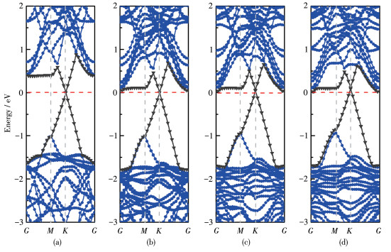
Figure 4 Energy band structures of (a) monolayer BP with the HSE06 method, (b) monolayer BP with the GGA-PBE method, (c) graphene and (d) BP/Gr heterostructure
The n-type (p-type) SBH are indicated between the Femi level and the conduction band minimum (the valence band maximum) of the BP monolayer; the Fermi level is set to zero and marked by red dotted lines.

Figure 5 Energy band structure of BP/Gr heterostructures with different proportions of the $\mathrm{O}$ atom doped: (a) $0 \%$; (b) $5.56 \%$; (c) $11.11 \%$; (d) $16.67 \%$

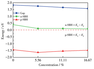
Figure 6 Dependence of SBH on different concentrations of the $\mathrm{O}$ atoms doped inside the layer
$E_{\mathrm{C}}, E_{\mathrm{V}}$ and $E_{\mathrm{F}}$ represent the CBM, VBM and Fermi level, espectively.

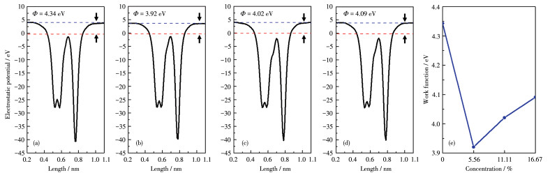
Figure 7 Calculated electrostatic potentials for (a) BP/Gr heterostructure, (b) BP/Gr-1O, (c) BP/Gr-20, (d) BP/Gr-30 and (e) plots of the $\mathrm{O}$ concentration on the work function tunability of BP/Gr heterostructures with $\mathrm{O}$ atoms doped inside the interface
The blue and red dashed lines denote the vacuum energy level and Fermi level, respectively.

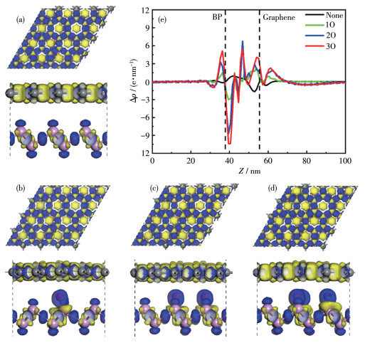
Figure 8 Top and side view of the 3D charge density difference for (a) BP/Gr heterostructure, (b) BP/Gr-10, (c) BP/Gr-20, (d) BP/Gr-30; (e) Planar electron density differences along the $z$ direction of BP/Gr heterostructures with different concentrations of the $\mathrm{O}$ adsorption doped inside the interface, in which positive and negative values represent electron accumulation and depletion in the space with respect to isolated BP and graphene, respectively
The isovalue chosen to plot the isosurface is $60 \mathrm{e} \cdot \mathrm{nm}^{-3}$.
Table 1. Mismatch energies and cohesive energies of BP/Gr heterojunctions with different proportions of the O-doped
| Heterojunction | Energy |
|||||||||||
| Mismatch | Cohesive | |||||||||||
| 0.327 | 0.327 | 0.247 | 0.247 | 0.98 | 0.98 | 0.714 | 0.714 | 0.3 | -1.4 | |||
| 0.327 | 0.327 | 0.247 | 0.247 | 0.983 | 0.984 | 0.714 | 0.714 | 2 | -5.8 | |||
| 0.327 | 0.327 | 0.247 | 0.247 | 0.984 | 0.983 | 0.714 | 0.714 | 2.4 | -9.2 | |||
| 0.327 | 0.327 | 0.248 | 0.248 | 0.983 | 0.985 | 1.121 | 1.121 | 11.9 | -10.6 | |||
 下载: 导出CSV

 扫一扫看文章

扫一扫关注我们