Citation:
Wenxue Zhang, Jiating Hou, Min Bai, Cheng He, Jiuran Wen. Spontaneously enhanced visible-light-driven photocatalytic water splitting of type Ⅱ PG/AlAs5 van der Waal heterostructure: A first-principles study[J]. Chinese Chemical Letters,
2023, 34(12): 108270.
doi:
10.1016/j.cclet.2023.108270
Spontaneously enhanced visible-light-driven photocatalytic water splitting of type Ⅱ PG/AlAs5 van der Waal heterostructure: A first-principles study
English
Spontaneously enhanced visible-light-driven photocatalytic water splitting of type Ⅱ PG/AlAs5 van der Waal heterostructure: A first-principles study
Received Date:
10 January 2023 Accepted Date:
23 February 2023 Revised Date:
07 February 2023 Available Online:
15 December 2023
Abstract:
To solve the problem of energy scarcity and widespread environmental contamination, it is necessary to design green and low-cost photocatalysts for water splitting. In this paper, a new penta-graphene/AlAs5 (PG/AlAs5) van der Waals (vdW) heterostructure is proposed and its performance for photocatalytic hydrolysis is calculated using the first-principles method. The findings suggest that the PG/AlAs5 heterostructure belong to type-Ⅱ indirect semiconductor, and the edge position and band gap width of this heterostructure satisfy the requests of redox reaction. Furthermore, the oxidation reaction (OER) on the AlAs5 side and the hydrogen evolution reaction (HER) on the PG side are thermodynamically spontaneous under different conditions. Surprisingly, the introduction of strain engineering has changed the position of the band edge and light absorption performance of PG/AlAs5 heterostructure, which is powerful for the performance of photocatalytic water splitting. The PG/AlAs5 vdW heterostructure exhibits well visible light absorption intensity without applying strain and biaxial strain of 2%. In conclusion, the findings suggest that the PG/AlAs5 vdW heterostructure is a prospecting catalyst for visible-light hydrolysis.
The large-scale use of fossil fuels has seriously undermined environmental sustainability. It can also be harmful to people's lifestyles and physical fitness. With the environment and energy sources being severely damaged, human beings urgently need to find pollution-free green and low-carbon energy to solve this problem [1–4]. So far, the use of water splitting to produce hydrogen is a very common way to solve the energy crisis [5–9]. It has the benefit of promising, and no additional contaminants [10]. Recent years, many monolayer semiconductor materials have been considered as hydrolytic photocatalysts that can generate hydrogen gas, such as TiO2 [11,12], ZnO [13,14], CuO [15,16]. Based on the theory of hydrolysis photocatalysis, the ideal photocatalyst should not only have the characteristics of low price, nontoxic and stable structure [17,18], but also meet the narrow band gap width, high carrier mobility, suitable band edge position orientation, and strong redox ability [19,20]. However, most one-component photocatalysts have the disadvantages of low visible light absorption rate and high electron-hole recombination rate, which restricts the application of hydrolytic photocatalysts in real-life applications [21]. Therefore, it is necessary to find a semiconductor photocatalyst that can spontaneously and efficiently split water under visible light exposure.
Two-dimensional (2D) materials have excellent special features such as high carrier mobility, short carrier migration distances, and large specific surface area. Therefore, 2D materials are widely used in the study of photocatalytic hydrolysis [22–24]. In 2004, K. S. Novoselov et al. [25] successfully prepared graphene by mechanical peeling method, and its application areas are expanding accordingly. Graphene occupies an important application prospect in the fields of materials and energy because of its excellent chemical stability, non-toxicity and excellent photoelectricity [26], but graphene cannot be used as a catalyst for hydrolysis due to its presence of a Dirac cone in the band structure. In recent years, defective materials can exhibit outstanding performance [27]. Topological defects in carbon nanomaterials (pentagons, heptagons, etc.) is able to exhibit completely different electronic properties when compared to graphene. Yan et al. [28] have demonstrated that carbon-based materials with pentagonal structure can be used as the main active site of oxygen reduction reaction (ORR) because of its electronic structure. From the results obtained from electrochemical tests, it is further proved that the defects of pentagon-based graphene have a more stimulating effect on catalytic oxygen reduction activity than graphene with ordinary hexagonal structures [27]. Cheng et al. [29] have performed high-temperature cyclic dehydrogenation on Au(111) and discovered pentagon-graphene by surface synthesis. And a series of tests is proved its potential electronic properties. However, PG has a wide band gap of up to 3 eV and the separation rate of photo-generated carriers is not high, which still hinder the application of single-molecular layer pentacyclic graphene in water splitting photocatalysts [30].
In fact, constructing heterostructure [31–33] can be used to adjust its properties to facilitate the use as water splitting catalysts. Zhang et al. [34] have proved that PG/GeP2 and PG/SiP2 heterostructures exhibit unique charm in the field of photocatalytic water splitting. And group Ⅲ-Ⅴ compounds are widely used in batteries, catalysts and other fields because of their peculiar structure and high carrier mobility [35]. Gao et al. [36] have studied the group Ⅲ-Ⅴ compounds by DFT calculations, which have proved that the Ⅲ-Ⅴ semiconductors have excellent mechanical and piezoelectric properties. Liu et al. [37] have demonstrated that graphene combined with Ⅲ-Ⅴ semiconductors could induce quenching of optical phonons and play an important role in optoelectronics and electronic devices. In recent years, five potential AlAs phases have been reported to determine their structural stability, mechanics, and thermomechanical properties [38]. M. D. Efremov has proposed that a molecular-beam epitaxy growth could be used on the semi-insulated GaSe(001) to generate GaAs0.6/AlAs5 superlattice [39]. Group Ⅲ-Ⅴ compounds are widely used in photocatalytic water splitting due to their excellent electron mobility. It has been reported that photogenerated electrons and holes accumulate on different monolayers in type Ⅱ heterostructure to achieve the purpose of electron and hole separation. This further completes the subsequent redox reaction. Therefore, by constructing a type Ⅱ heterostructure is one of the valid methods to prepare hydrolytic photocatalysis [40,41]. Cui et al. [42] confirmed that the g-GaN/TMD heterostructure can be applied to the field of water splitting by the study of first functional theory. Other studies have also shown that the group Ⅲ-Ⅴ compounds (such as AlAs/SiH [43], GaP/GaAs [44], GaAs/SiH [45]) could form type Ⅱ heterostructure and be used as photocatalytic water splitting materials. However, the band gap width of the Ⅲ-Ⅴ semiconduction is not fixed, and the band gap width of GaAs and AlAs is only 2.06 eV and 4.05 eV [43,45]. PG band gap is so wide that the absorption of visible light is not ideal. Therefore, a type-Ⅱ vdW heterostructure based on PG and AlAs5 semiconductor (PG/AlAs5) are considered to design as a photocatalyst in this paper. And it is discussed whether it can effectively inhibit electron and hole compounding or not, thereby achieving a clean water splitting catalyst.
Herein, the energy band structure, density of states, band edge positions and optoelectronic natures of the PG/AlAs5 heterostructure are specifically calculated using density functional theory (DFT). The outcomes show that the PG/AlAs5 heterostructure is an indirect semiconductor with a band gap of 2.13 eV, and its band edge position and optical absorption coefficient satisfie the photo-catalytic hydrolysis request. In addition, the variations of band structure and the position of the band edges of the structure after the addition of small amplitude strain are systematically studied. Subsequently, according to the calculation of Gibbs free energy, the thermodynamic properties of PG/AlAs5 heterostructure in the process of adsorption of water molecules are analyzed. In conclusion, the results show that PG/AlAs5 heterostructure can be used as photocatalysts.
This paper is based on DFT, theoretical calculations are performed using Vienna Ab initio Simulation Package (VASP) and Projected Augmented Wave (PAW) methods [46]. The exchange-correlation potential is specifically calculated using the generalized gradient approximation of the Perdew-Burke-Ernzerhof (GGA-PBE) generalized function [47,48]. The electronic character of the heterostructure uses the more accurate HSE06 [49] hybrid function method. Furthermore, the optical properties were compared using a conjunction of the GW approximation [50] and the Bethe-Salpeter equation (BSE) [51] with a conjunction of the GW approximation and the random phase approximation (RPA) [52]. The van der Waals interactions between monolayer PG and AlAs5 after forming a heterostructure can be corrected with the DFT-D2 correction method in the Grimme's scheme [53]. In the calculation process the cut-off energy of the plane wave is 400 eV, the convergence tolerance of the energy is chosen to be 1 × 10⁻⁵ eV, and the maximum residual force was fixed to 0.03 eV/Å. In addition, the Brillouin zone was sampling using a 4 × 4 × 1 Monkhorst-Pack k-point mesh. When the structure was optimized, a vacuum buffer space of 25 Å was added to separate the interlayer interactions caused by periodicity.
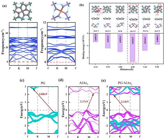
The lattice parameter of PG monolayers after structural optimization is 3.64 Å. This is in agreement with the previously reported findings [30]. The researchers have confirmed that the lattice parameters of the AlAs of zinc-blende structure and rocksalt structure are 5.67 Å and 5.38 Å, respectively [54]. Liu et al. successfully confirmed that BP5 is a penta-graphene-like 2D stable structure with a tetragonal lattice through theoretical simulation [55]. Inspired by these, an AlAs5 monolayer was constructed. As shown in the top view of predicted structure of penta-AlAs5 monolayer in Fig. S1 (Supporting information), and the structure have a tetragonal lattice and is constructed of pentagonal structures. Its symmetry space group is P-4 (No. 81) and its structure-optimized lattice parameter is 5.17 Å. The Al atom located in the middle of 5 As atoms, and the "thickness" of the sheet is observed in the top view of AlAs5 as 3.90 Å. The phonon spectra of the nanolayer of PG and AlAs5 structures are shown in Fig. 1a, and the absence of imaginary frequencies in the phonon spectra confirms the dynamic stability of the two structures.
Figure 1
Figure 1.
(a) The phonon dispersion curve of nanolayer of PG and AlAs5. (b) Top and side view of different stacking patterns, binding energies, and distances of the PG/AlAs5 Each atom of PG is marked. The most stable stacking pattern is indicated by a red frame. Gray represents C atoms, lilac represents As atoms, and orange represents Al atoms. (c-e) Band structures of monolayers PG and AlAs5 and PG/AlAs5 heterostructure. The Fermi level is set to zero.
Then, the optimized PG and AlAs5 monolayers are superimposed vertically under vdW interaction to obtain the PG/AlAs5 vdW heterostructure. In order to minimize the effects of lattice mismatch, PG nanolayer with and AlAs5 nanolayer with 1 × 1 × 1 pile up into the PG/AlAs5 heterostructure. After optimization, the lattice parameter of the newly combined heterostructure is 5.16 Å, and its relative lattice mismatch rate is measured as 0.04%. Due to the formation of heterostructure between different C atoms in PG and AlAs5, the structural stability of the construction is different. In order to select the most stable stacking mode. The C atoms in the PG monolayer are labeled 'C1', 'C2', 'C3', 'C4', 'C5'. Therefore, six different stacked structures of the PG/AlAs5 heterostructure are constructed and labeled them as Al-C1, Al-C2, Al-C3, Al-C4, Al-C5 and Al-h, respectively. The character 'h' represents that Al atom is located at the center of PG. In order to select the most stable stacking mode, the binding energy Eb of the structure is calculated as follows:
(1)
Among them, Eheterostructure, Emonolayer1, Emonolayer2 represent the total energies of PG/AlAs5 heterostructure, pristine PG monolayer and pristine AlAs5 monolayer after geometry optimization, respectively. Different stacking patterns are considered to have an effect on the magnitude of the binding energy. Binding energies and layer spacings for six different stacking patterns are shown in Fig. 1b. It can be seen that the Al-h stacking pattern of PG/AlAs5 heterostructure has a minimum Eb of −0.023 eV and layer spacing of 4.86 Å. Furthermore, the phonon dispersion curve of the Al-h stacking PG/AlAs5 heterostructure is calculated (Fig. S2b in Supporting information). No virtual frequency confirms its stability. Therefore, this stacking pattern is the most stable and should be used to study the hydrolysis properties of PG/AlAs5 heterostructure.
After selecting the stable structure of the PG/AlAs5 heterostructure, its electrical characteristics have also been studied. The band structure diagram of the single-layer PG, single-layer AlAs5, and PG/AlAs5 heterostructure computed by the HSE06 functional is shown in Figs. 1c-e. And the electrostatic potential data among the pristine PG monolayers, pristine AlAs5 monolayer, and PG/AlAs5 vdW heterostructure is shown in Table 1. PG and AlAs5 are indirect semiconductors with bandgaps of 3.04 and 2.17 eV, respectively. In Fig. 1e, the minimum conduction band (CBM) of the PG/AlAs5 heterostructure is between points Γ and the K, and the valence band maximum (VBM) of the PG/AlAs5 heterostructure is situated between point K and point M, so it belongs to the indirect bandgap semiconductor. The band width of the PG/AlAs5 heterostructure decreases to 2.13 eV when two single nanolayers combine to form a heterogeneous structure. Most of the CBM of the heterostructure is mostly provided by the single-layer PG, of which AlAs5 is also present in small amounts in CBM, and the VBM is only provided by the single-layer AlAs5. When the sunlight shines on the PG/AlAs5 heterostructure, the electrons in the VB are excited to the CB. Photogenerated electrons and holes can be efficiently separated and aggregated on different monolayers.
Table 1
Table 1.
Calculated electrostatic potential at the Fermi level Ef, the electrostatic potential in a vacuum near to the surface Evac, band gap Eg, work function (Φ) in comparison for PG, AlAs5 and PG/AlAs5 vdW heterostructure with Al-h stacking.
This is followed by an in-depth exploration of the density of states (DOS) and the partial density of states (PDOS). On the negative semi-axis of Fig. S2a (Supporting information), the peaks of the AlAs5, and PG/AlAs5 heterostructure first appear in the form of interactive superposition. On the positive half axis, both PG and AlAs5 overlap with the peak of the PG/AlAs5 heterostructure. From this, the PG/AlAs5 heterostructure can also be determined as a type Ⅱ heterostructure. The heterostructure of PG/AlAs5, the VBM is contributed from the p-orbital of the As atom in the AlAs5 layer. On the other hand, CBM are mainly contributed by multiple orbitals in the AlAs5 layer. The identification of this type Ⅱ heterostructure offered the basis for follow-up photocatalytic studies of water splitting.
To further understand the charge transfer and redistribution inside the PG/AlAs5 heterostructure. Therefore, the difference in charge density (Δρ) is introduced, the formula is as follows:
(2)
Among them, Δρ(z)heterostructure indicates the charge density of the PG/AlAs5 heterostructure, and Δρ(z)monolayer1 and Δρ(z)monolayer2 delegate the charge densities of monolayer PG and AlAs5, respectively. A positive value of Δρ indicates the accumulation of charge here, while a negative value indicates the loss of charge. In addition, the dipole moments indicates the generation of interfacial dipoles at the interface. The dipole moment is represented by the equation as follows:
(3)
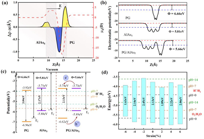
From Fig. 2a, in the PG/AlAs5 heterostructure, the single-layer AlAs5 is negative and the single-layer PG is positive. This represents the charge shift from AlAs5 to the PG layer, so the holes are allocated in AlAs5and electrons are allocated in PG. In addition, the dipole moment of the PG/AlAs5 heterostructure is 1.25 D. This also indicates that an interfacial dipole is generated at the interface of the heterostructure, and the direction of the electric field is pointed from AlAs5 to the PG layer. In addition, the electrostatic potential distribution of PG/AlAs5 heterostructure and single nanolayers PG and AlAs5 in the Z direction is shown in Fig. 2b. And work function (Φ) of the original PG monolayer, AlAs5 monolayer, and PG/AlAs5 heterostructure are 6.66 eV, 5.81 eV, and 5.66 eV, respectively. This indicates that the AlAs5 layer is more prone to electron loss. In addition to studying Δρ, bader charge can reflect the gain and loss of charge for each atom, so the charge transfer can be seen more intuitively. From the charge analysis of the PG/AlAs5 heterostructure in Fig. S2c (Supporting information), it can be seen that the charge of the C atom is positive and the charge of the Al and As atoms are negative, revealing that the electron transfer is from AlAs5 to PG, which is in agreement with the results obtained for Δρ.
Figure 2
Figure 2.
(a) Planar average charge-density difference and interfacial dipole moment along the Z direction for the PG/AlAs5 heterostructure. (b) The electrostatic potential along the Z-direction of pristine PG monolayer, pristine AlAs5 monolayer, and PG/AlAs5 vdW heterostructure. The red dotted line represents the vacuum level and the blue dotted line represents the Fermi level. (c) Potential band-edge position of monolayers PG, AlAs5, and the PG/AlAs5 heterostructure. (d) Effect of applied strains of −6%, −4%, −2%, +2%, +4% and +6% on the band gaps (Eg). The black, brown, and green dashed lines are the water redox potentials at pH 0, 7 and 14, respectively.
Excellent hydrolysis photocatalysts, besides having excellent band gap to absorb visible light, the band edge positions are also needed to be suitable for OER. The conductive band (CB) ought to be located at an electrostatic potential above the reduction potential H+/H2, and the valence band (VB) should be lower than the oxidation potential O2/H2O [56]. As we all know, the standard potentials of H+/H2 (EH+/H2) and O2/H2O (EO2/H2O) are −4.44 and −5.67 eV at pH 0, respectively [56]. EH+/H2 and EO2/H2O can be expressed at other pH values [2]:
(4)
(5)
Fig. 2c shows the position of the electrostatic potential at the PG/AlAs5 heterostructure. As a result, the CBM and VBM edge positions of PG are −3.92 and −6.96 eV, respectively, with respect to the normal hydrogen electrode (NHE). Similarly, the position with edge of AlAs5 are −3.71 and −5.88 eV, respectively. The high carrier recombination of the monolayer photocatalytic material reduces its catalytic efficiency, so the position of the energy edge after forming a heterostructure is discussed. The position of the band edge will change after two monolayers form a heterostructure structure. The edge positions of the PG/AlAs5 heterostructure are −3.74 and −5.89 eV, separately. CBM is above all EH+/H2 values in the pH range of 0-7, and VBM is lower than all EO2/H2O standard potentials in the pH range of 0-7. This band arrangement is similar to some of the previously reported type Ⅱ heterostructure photocatalysts, such as h-BN/C2N [41], InSe/SiH [40], ZnO/BSe [57]. The results show that the PG/AlAs5 heterostructure could occur under both acidic and neutral conditions. Thus, the electrons are travelling from AlAs5 to PG, while the holes are transferred from PG to AlAs5.
The PG/AlAs5 heterostructure of CBM and VBM are located to meet the demands of photocatalytic hydrolysis. Numerous works have shown as well by applying biaxial strain can change the position with band edge and thus better absorb visible light [34]. Thus, as described in this paper, by studying the changes in the band position and light absorption of PG/AlAs5 heterostructure after strain application, and judging whether it is more suitable for hydrolysis. Biaxial strain (ε) is calculated by the formula ε = Δa/a0, where a0 is the lattice parameter of the unstretched original structure in equilibrium and Δa is the difference between the original unstretched lattice parameter and the tensile lattice parameter. ε < 0 and ε > 0 represent compression and stretch, respectively [58]. After the application of biaxial strain, no structural deformation occurred in the PG/AlAs5 heterostructure. Therefore, the changes in band gap width and band edge position of PG/AlAs5 heterostructure are investigated when applying +2%, +4% and +6% biaxial tensile strains and −2%, −4% and −6% biaxial compression strains. As described in Fig. S3 (Supporting information), when a biaxial compression strain is imposed, the gap width of the PG/AlAs5 heterostructure increases firstly and then decreases as the strain increases. Conversely, when a biaxial tensile strain is applied, the band gap width of the PG/AlAs5 heterostructure decreases firstly and then increases and then decreases as the strain increases. Regardless of whether compressive strains or tensile strains are applied or not, The PG/AlAs5 heterostructure remains an indirect bandgap semiconductor. It is surprising that when +4% and +6% strains are applied, both CBM and VBM of the PG/AlAs5 heterostructure are provided by AlAs5. The magnitude of the effect of the applied biaxial strain on the edge position of the PG/AlAs5 heterostructure band is discussed (Fig. 2d). When applying −2% or −4% compression strain, the band edge position of the PG/AlAs5 heterostructure under neutral and acidic conditions meets the requests for hydrolysis. Surprisingly, the PG/AlAs5 heterostructure could satisfy the request for hydrolysis under alkaline conditions when a −2% strain is applied. The PG/AlAs5 heterostructure at strain of +4% and +6%, the band edge position is straddle EH+/H2 and EO2/H2O in neutral and acidic positions. So the PG/AlAs5 heterostructure after applying +2% or −2% strains is still suitable for water splitting reactions.
Excellent carrier mobility are also required for efficient photocatalysts. The smaller the effective mass of the carriers the more beneficial their migration. So the effective mass of the electron-hole of the PG/AlAs5 heterostructure needs to be studied. In Fig. S2d (Supporting information), the effective masses of holes (mh) and electrons (me) of the PG/AlAs5 heterostructure without strain are 2.15 m0 and 0.51 m0, respectively. The value of mh is much larger than me. At this time, applying a biaxial strain is considered to adjust the gap. When a + 2% tensile strain is applied to the heterostructure, the me grows significantly to 2.21 m0, at which point the mh is 1.47 m0. Therefore, strain engineering has a forceful impact on the effective masses and band edge position of PG/AlAs5 heterostructure.
By studying the electrical properties of the PG/AlAs5 heterostructure, it can be proved that the PG/AlAs5 heterostructure can undergo water-splitting reactions. Next, the attraction of water elements on heterostructure is studied to judge whether it can spontaneously occur in thermodynamic terms. Based on the energy band structure analysis in the previous section, HER occurs on the electron aggregation side and the OER happens on the hole aggregation side. HER reaction is located at the cathode:
(6)
As well as more complex OER occurs at the anode:
(7)
(8)
(9)
(10)
Among them, * represents PG/AlAs5 heterostructure bases, while OH*, O* and OOH* stand for small elements attracted to heterostructure. The reaction schematic is shown in Fig. S4a (Supporting information). The reaction of PG/AlAs5 heterostructure at strains of +2% or −2% is also discussed. The changes of free energy (ΔG) of the elementary steps are based on the equation below [59]:
(11)
Among them, ΔE represents the change in total energy and ΔZPE expresses the fluctuation of zero-point energy. ZPE is given as following formula:
(12)
The vibration frequency is denoted by vi. ΔS denotes the entropy contribution at T = 298.15 K, and TS is represented as follows:
(13)
where kb is to denote the Boltzmann constant, and e and h are the electron charge and Planck constant, respectively. In addition, the change brought by the electrode potential to the ΔGU of the reaction can be given by the following equation:
(14)
The electrode potential U is expressed using the difference between the VBM and EH+/H2 in the OER and the difference between the CBM and EO2/H2O in the HER. The change in ΔG (ΔGpH) brought about by the pH value may be described as:
(15)
(16)
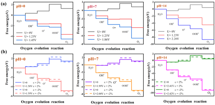
The ΔG oxidation reaction of PG/AlAs5 heterostructure is calculated, and the thermodynamic possibilities under acidic (pH 0), neutral (pH 7), and alkaline (pH 14) conditions are calculated, respectively. The thermodynamic possibility of HER occurrence on the PG nanolayer is shown in Fig. S4b (Supporting information). The results of ΔG show that HER can spontaneously perform thermodynamic processes under acidic and neutral conditions when HER is applied at U = 0.7 V or U = 0.29 V, respectively. Compared to HER, OER is a more complex process involving four electron transfers. Fig. 3 shows the ups and downs of free energy of the PG/AlAs5 heterostructure in different situations. PG/AlAs5 heterostructure at a value of 0 for both pH and U (Fig. 3a), the first three steps of ΔG are increasing. When U = 1.23 V is imposed on this basis, the ΔG decreases significantly per step, but there is still an increasing of ΔG. After applying U = 1.45 V, the ΔG decreases at each step. This shows that the OER of the PG/AlAs5 heterostructure proceeds smoothly at 1.45 V from a thermodynamic point of view. The PG/AlAs5 heterostructure with a pH of 7 and U = 0, U = 1.23 V has a phenomenon of free energy increase. When U = 1.86 V is applied, there is a tendency for ΔG to reduce at each step. This suggests that from a thermodynamic point of view, the OER of the PG/AlAs5 heterostructure can be carried out spontaneously at U = 1.86 V. When the pH is 14 without applied optical voltage, only the first step ΔG decreases. Immediately following, 2.28 V is applied, and PG/AlAs5 heterostructure can spontaneously perform OER. When the last step of the OER, U = 2.28 V, G = −8.66 eV.
Figure 3
Figure 3.
Gibbs free energy (ΔG) diagrams of the OER occurring on the surface of (a) PG/AlAs5 heterostructure and (b) PG/AlAs5 heterostructure with +2% and −2% strain applied at pH 0, 7 and 14, respectively.
In addition, to study the effect of small biaxial strains on ΔG, the ΔG of each basic step of PG/AlAs5 (−2%) and PG/AlAs5 (+2%) is calculated (Fig. 3b). From the graph, we can understand that the PG/AlAs5 heterostructure cannot meet the thermodynamic conditions of OER by only applying biaxial strain at pH 0, 7 and 14. For the PG/AlAs5 heterostructure in Fig. 3b, the OER of 2.00 and 2.42 V at pH 7 and 14 under compression strain of −2%, the ΔG of each step of the heterostructure showed a significant downward trend. At the time when the exerted tensile strain is +2%, the heterostructure of OER could be carried out smoothly at pH 0/7/14 and voltages of 1.58/1.99/2.41 V. It can be seen that the OER reaction of the PG/AlAs5 heterostructure can be carried out spontaneously at any pH value. It follows that the PG/AlAs5 heterostructure could withstand small strains at any pH value, and the OER reaction proceeds smoothly under thermodynamic conditions. Therefore, after applying the stresses of −2% and +2%, the OER can also undergo thermodynamic reactions at pH 7 and 14, and the PG/AlAs5 van Der Waals heterostructure with stress of −2% and +2% can effectively catalyze water splitting.
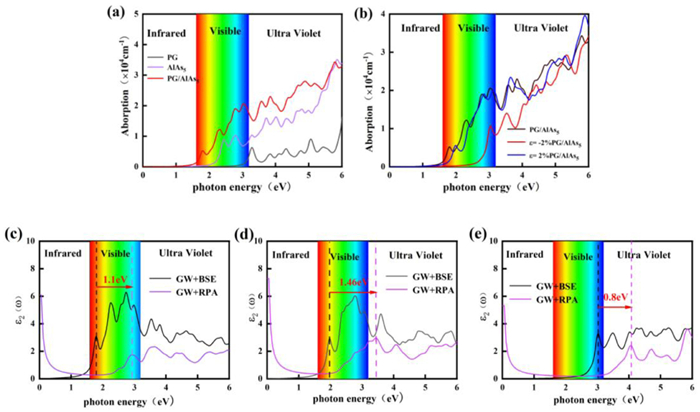
Having a good visible light absorption rate is one of the conditions for excellent photocatalysts. It has been shown that the application of −2% and +2% biaxial strains improves the performance of photocatalytic water splitting. Therefore, the visible absorption coefficients of monolayer PG and AlAs5 and PG/AlAs5 heterostructure are shown in Fig. 4a. It shows that the peak of the heterostructure has increased significantly compared with PG and AlAs5 nanolayers, and the redshift phenomenon occurs. The results show that the synthesis of heterogeneous structures is beneficial to the absorption of visible light. The difference in the light absorption coefficients of the PG/AlAs5 heterostructure without and after applying strain can be viewed in Fig. 4b. It can be seen from the figure that the visible light absorption coefficient of the +2% biaxial tensile strain is almost the same as that of the unstrain state. But the imposition of the −2% compression strain reduces the absorption coefficient of the visible light. Therefore, it is argued that the introduction of strain engineering has a moderating effect on the response of natural light.
Figure 4
Figure 4.
Optical absorption spectra of (a) pristine PG monolayer, pristine AlAs5 monolayer, and PG/AlAs5 heterostructure (b) PG/AlAs5, PG/AlAs5 (−2%) and PG/AlAs5 (+2%). Optical absorption spectra of monolayers (c) PG/AlAs5 and (d) PG/AlAs5 (+2%), and (e) PG/AlAs5 (−2%) heterostructure.
Additionally, two algorithms, GW+BSE and GW+RPA, are used to clarify the optical characteristics in PG/AlAs5 heterostructure. The light absorption map obtained by GW+RPA algorithm lacks the influence of exciton binding energy, while GW+BSE considers the effect of exciton binding energy on electron holes on recombination. So it is more accurate to use GW+BSE. In Fig. 4c, the exciton binding energy is defined as the gap from the absorption peak between the two methods of calculation. In general, the higher the exciton binding energy, the more likely the photogenerated electrons and holes will bind, which is detrimental to the photocatalyst. Analysis of the imaginary part of dielectric constant of the PG/AlAs5 heterostructure without strain and after the application of +2% and −2% strain are shown in Figs. 4c-e. As shown in Fig. 4e, the binding energy of the exciton after applying a −2% biaxial compressive strain is reduced to 0.8 eV. However, a significant decrease in the number of absorption peaks and a decrease in the absorption coefficient are observed in the visible region.
In summary, the optoelectronic properties of PG/AlAs5 heterostructure with secondary type Ⅱ were investigated by DFT, and their potential use as water splitting photocatalysts was explored. The most stable PG/AlAs5 heterostructure was selected, where the distance (d) is 4.86 Å and Eb is −0.023 eV. Then, the position of the band edge where the heterostructure is located satisfies the demand of hydrolysis. This proves that its redox reaction is thermodynamically spontaneous. Moreover, the introduction of strain can better catalyze the decomposition of water. Especially when the strain is +2%, the PG/AlAs5 heterostructure has the strongest light absorption capacity, which is beneficial to improve the property of photocatalytic water splitting. At a compressive strain of −2%, the PG/AlAs5 heterostructure can meet the demands of water splitting at any pH value. Therefore, predicting the PG/AlAs5 heterostructure is an important candidate structure for photocatalytic water splitting.
Declaration of competing interest
The authors declare that they have no known competing financial interests or personal relationships that could have appeared to influence the work reported in this paper.
Acknowledgments
The authors acknowledge supports by National Natural Science Foundation of China (NSFC, No. 52271113), Natural Science Foundation of Shaanxi Province, China (Nos. 2019JM-189, 2020JM-218), the Fundamental Research Funds for the Central Universities (Nos. CHD300102311405, CHD300102312405), HPC platform, Xi'an Jiaotong University.
Supplementary materials
Supplementary material associated with this article can be found, in the online version, at doi:10.1016/j.cclet.2023.108270.
H. Wang, H. Yuan, S. Sae Hong, et al., Chem. Soc. Rev. 44 (2015) 2664–2680. doi: 10.1039/C4CS00287C
[59]
Y. Yu, J. Zhou, Z. Sun, Adv. Funct. Mater. 30 (2020) 2000570. doi: 10.1002/adfm.202000570
Figure 1
(a) The phonon dispersion curve of nanolayer of PG and AlAs5. (b) Top and side view of different stacking patterns, binding energies, and distances of the PG/AlAs5 Each atom of PG is marked. The most stable stacking pattern is indicated by a red frame. Gray represents C atoms, lilac represents As atoms, and orange represents Al atoms. (c-e) Band structures of monolayers PG and AlAs5 and PG/AlAs5 heterostructure. The Fermi level is set to zero.
Figure 2
(a) Planar average charge-density difference and interfacial dipole moment along the Z direction for the PG/AlAs5 heterostructure. (b) The electrostatic potential along the Z-direction of pristine PG monolayer, pristine AlAs5 monolayer, and PG/AlAs5 vdW heterostructure. The red dotted line represents the vacuum level and the blue dotted line represents the Fermi level. (c) Potential band-edge position of monolayers PG, AlAs5, and the PG/AlAs5 heterostructure. (d) Effect of applied strains of −6%, −4%, −2%, +2%, +4% and +6% on the band gaps (Eg). The black, brown, and green dashed lines are the water redox potentials at pH 0, 7 and 14, respectively.
Figure 3
Gibbs free energy (ΔG) diagrams of the OER occurring on the surface of (a) PG/AlAs5 heterostructure and (b) PG/AlAs5 heterostructure with +2% and −2% strain applied at pH 0, 7 and 14, respectively.
Table 1.
Calculated electrostatic potential at the Fermi level Ef, the electrostatic potential in a vacuum near to the surface Evac, band gap Eg, work function (Φ) in comparison for PG, AlAs5 and PG/AlAs5 vdW heterostructure with Al-h stacking.

 DownLoad:


 下载:
下载:


