Citation:
Xiaoyang Du, Qian Zhang, Zeyu He, Hui Lin, Gang Yang, Zhenhua Chen, Caijun Zheng, Silu Tao. Performance enhancement in organic solar cells and photodetectors enabled by donor phase optimization at the surface of hole transport layer[J]. Chinese Chemical Letters,
2023, 34(6): 107641.
doi:
10.1016/j.cclet.2022.06.064
Performance enhancement in organic solar cells and photodetectors enabled by donor phase optimization at the surface of hole transport layer
English
Performance enhancement in organic solar cells and photodetectors enabled by donor phase optimization at the surface of hole transport layer
Received Date:
30 April 2022 Accepted Date:
23 June 2022 Revised Date:
13 June 2022 Available Online:
15 June 2023
Abstract:
The domain purity, material crystallinity and distribution at the interface between the active layer and the transport layer have an important impact on the performance of organic solar cells (OSCs) and organic photodetectors (OPDs), while this focal issue has received less attention in previous studies. From this perspective, a new method to simultaneously enhance the performance of OSC and OPD is proposed, namely, using a sequential deposition method to first construct a compact stacking structure of dual-donor (D18-Cl:PTO2) eutectic in the donor layer, and then induce the ordered deposition of the acceptor (Y6). Compared with the conventional bulk heterojunction (BHJ), the active layer realized by this method not only improves the crystallinity and stacking order of the constituent material on the surface of the transport layer, but also regulates a good vertical distribution, which is conducive to improving the charge transport and extraction efficiency, reducing the leakage current, and enhancing the stability of the device. As a result, the OSC device based on the D18-Cl:PTO2/Y6 structure achieves a power conversion efficiency of up to 17.65% and good light-degradation stability, which is much better than that of BHJ-based OSC (PCE of 16.37%). For the OPD, the dark current at reverse bias is reduced by more than an order of magnitude, and the maximum responsivity is improved to 0.52 A/W through the optimization of the donor phase at the interface. Moreover, the strategy does not require additional post-processing compared to the BHJ preparation, which reduces the device construction cost and process complexity, providing an effective way for developing high-performance organic optoelectronic devices.
Organic optoelectronic devices based on organic semiconductor materials have attracted widespread attention and research interest due to their advantages of flexibility, light weight and environmentally friendly [1-6]. Among the organic optoelectronic devices, organic solar cells (OSCs) and organic photodetectors (OPDs), which can convert light into electricity, featuring advantages of broad class of materials, easy adjustment of energy level and solutions processability, and are considered to be a popular research topic and focus in recent years [7-16]. Conventional OSCs and OPDs were developed from diode structures based on bulk heterojunctions (BHJs) [17-19]. Contributing to the continuous development of high performance organic semiconductor materials in recent years, the efficiency of BHJ-based single-junction OSCs has reached 19%, and the corresponding OPDs have achieved high sensitivity and broad spectral response for photodetection and medical applications [20-25].
However, organic optoelectronic devices based on BHJ structure still have some inherent issues that limit the further development of device performance and hinder the industrialization process of organic optoelectronic devices. On the one hand, the micro-morphology of the BHJ, the crystallization and stacking characteristics of the component materials are difficult to control, especially the material distribution and phase domain continuity of the BHJ in the vertical direction usually need to be realized with the help of additional treatments, such as additive strategies, saturated solvents annealing, thermal annealing and other methods in concert [26-28]. This not only raises the device construction costs, but also imposes stringent requirements on the device preparation process. On the other hand, due to the homogeneous distribution of donor and acceptor materials in BHJ, it is inevitable that they are directly contacted with the transport layer, which greatly increases the chance of charge injection from external circuit to the device under the reverse bias and results in enhanced dark current and reduced detection performance [29-31]. These suggest that the crystallinity and ordered stacking of the materials at the interface between the active layer and the transport layer and the continuous material distribution in the vertical direction have a very important impact on the device performance. Focusing on this issue, researchers have proposed that using sequential deposition method to construct OSCs and OPDs can effectively regulate the vertical distribution of active layer materials [32-34]. However, the essential relation between the crystallization and stacking properties of active layer materials at the interface and device performance has been less studied in above researches. Clarifying the relationship between them is of great scientific importance for the construction of high-performance organic optoelectronic devices.
With this issue as the focus, we propose a new method to simultaneously improve the performance of OSCs and OPDs, that is introducing PTO2 molecules in the donor phase (D18-Cl:PTO2) as the first layer of sequential deposition process [35,36]. As PTO2 processes similar backbone structure with D18-Cl, D18-Cl:PTO2 blends can form highly crystalline, orderly stacked donor layer on the surface of the hole transport layer before spin-coating the acceptor solution. The enhanced crystallization and stacking characteristics of donor layer have the potential to induce orderly deposition of the acceptor material (Y6) when spin-coating the next layer [37]. Compared with the conventional active layer films based on the BHJ structure, this method can not only improve the crystallization and stacking characteristics of the component materials at the surface of the hole transport layer (PEDOT:PSS), but also effectively regulate the vertical distribution of the active layer materials, thus improving the transport and extraction efficiency of the photogenerated carriers, suppressing the unfavorable charge injection from the external circuit, and realizing high-performance organic optoelectronic devices. As a result, the OSC devices based on D18-Cl:PTO2/Y6 obtained a power conversion efficiency (PCE) of up to 17.65% and excellent light-degradation stability, which is much better than the binary and ternary OSCs based on the BHJ structure. In terms of OPD, the device constructed by this method achieved more than an order of magnitude decrease in dark current under the reverse bias and a maximum responsivity of 0.52 A/W. Moreover, the method does not require any additional post-treatment compared to the construction of high-performance BHJ. Therefore, the method presented in this work can improve the performance of organic optoelectronic devices while reducing the cost and complexity of device preparation, which is an effective strategy to realize high performance optoelectronic devices.
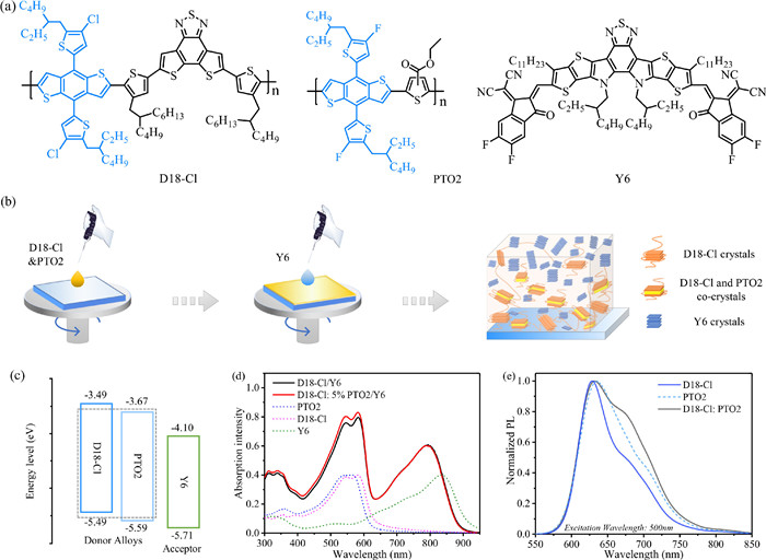
The molecular structure of the materials used to construct the active layer/photosensitive layer of the optoelectronic devices are shown in Fig. 1a, the donors D18-Cl and PTO2 have similar skeleton structures (marked in blue), which provides the prerequisite for the formation of copolymeric crystals during the film formation process. Y6 is used as an acceptor to ensure efficient exciton dissociation and electron transport. The energy level diagram of the component materials is shown in Fig. 1c, compared with D18-Cl, PTO2 has a higher highest occupied molecular orbital (HOMO) energy level. Therefore, under the premise that the dual donor materials co-crystallize to form an alloy model, the energy level difference between the HOMO of donor and the lowest unoccupied molecular orbital (LUMO) of acceptor (ED, HOMO – EA, LUMO) increases, which is expected to enhance the open-circuit voltage (VOC) of the device. The sequential deposition (SD) process performed in this work is shown in Fig. 1b, D18-Cl and PTO2 were dissolved in chlorobenzene (CB) solution at a concentration of 6 mg/mL and stirred overnight, and then the blended solution was spin-coated on PEDOTPSS substrate as the first layer. Immediately afterwards, Y6 solution (chloroform (CF) solution, 9 mg/mL) was dropped on above film to form the active layer. Here, D18-Cl:PTO2/Y6 and D18-Cl/Y6 represent the optimized and control films performed with sequential deposition process. Significantly, this method is simple to prepare without additional additives or post-treatment processes compared to the conventional BHJ based films. More importantly, compared to BHJ films, the present method not only provides a significant vertical phase distribution, but also improves the crystallinity of the donors, which is important for improving the performance of organic optoelectronic devices. The absorption spectra of D18-Cl, PTO2, Y6, D18-Cl/Y6 and D18-Cl:PTO2/Y6 films are shown in Fig. 1d, it can be seen that the absorption of D18-Cl:PTO2/Y6 containing film is increased in the 500–600 nm range compared to D18-Cl/Y6 based film, which is attributed to the enhanced photon capture by the introduction of PTO2. However, the binary and ternary BHJ-based films exhibited very similar absorption spectra (Fig. S1b in Supporting information). This result indicates that the enhancement in absorption spectrum of D18-Cl:PTO2/Y6 containing film may include the contribution of the elevated crystallinity of the donor. Furthermore, the absorption spectra of D18-Cl and D18-Cl:5%PTO2 containing films were studied as shown in Fig. S1a (Supporting information), the introduction of PTO2 in D18-Cl enhanced the absorption intensity of the donor, which may be attributed to the increased crystallinity of the donor. To further investigate the effect of the introduction of PTO2 on the crystallinity of the donors, photoluminescence (PL) spectra (Fig. 1e) and melting enthalpy changes (Fig. S2 in Supporting information) of the monomer as well as the blends in different ratios. The shoulder emission of the PL spectra of the hybrid film (D18-Cl:PTO2 = 1:1) was enhanced under 500 nm light excitation, which implies an enhanced stacking of the two donors in the hybrid film. The melting enthalpy of D18-Cl, PTO2 and D18-Cl:PTO2 (1:1) samples were measured via differential scanning calorimetry (DSC) as shown in Fig. S2, the melting enthalpies of the three components were obtained by integrating the melting peaks as 48.83 J/g, 59.90 J/g and 58.64 J/g, respectively, which means that the strength of crystallinity is D18-Cl < D18-Cl:PTO2 < PTO2. Besides, more crystallinity analysis is discussed subsequently in the morphological analysis. The compatibility between D18-Cl and PTO2 was analyzed by measuring the surface energy via contact angle characterization. The contact angle images of D18-Cl and PTO2 performed with water (H2O) and methylene iodide (CH2I2) mediums are shown in Fig. S3 (Supporting information). By calculation, the surface free energies of D18-Cl and PTO2 were estimated to be 31.73 mN/m and 32.42 mN/m, respectively. Very similar values of surface free energy imply that D18-Cl and PTO2 possess good compatibility in the co-blended system.
Figure 1
Figure 1.
(a) Molecular structures of D18-Cl, PTO2 and Y6. (b) Schematic illustration of sequential deposition process. (c) Energy level diagrams of D18-Cl, PTO2 and Y6. (d) Absorption spectra of D18-Cl, PTO2, Y6, D18-Cl/Y6 and D18-Cl:PTO2/Y6 films. (e) PL spectra of D18-Cl, PTO2 and D18-Cl:PTO2 (1:1) films.
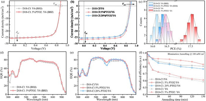
To investigate the contribution of the introduction of PTO2 to the performance of the optoelectronic devices, we prepared binary and ternary OSCs based on the BHJ structure and sequential deposition method, respectively. The OSC structure is ITO/PEDOT:PSS/Active layer/PDINN/Ag. For the OSC based on BHJ structure, D18-Cl, PTO2 and Y6 were dissolved in CF at a total concentration of 13 mg/mL and stirred overnight, then the solutions were spin-coated onto the substrate and annealed with CF saturated vapor atmosphere solvent for 5 min. And for the OSC fabricated by sequential deposition method, D18-Cl:PTO2 (6 mg/mL in CB solution) and Y6 (9 mg/mL in CF solution) were spin-coated on the substrate in sequence without any additional annealing process. PDINN was dissolved in methanol and deposited on active layer acted as electron transport layer [38]. The current density versus voltage (J-V) curves of the two types of OSCs are shown in Figs. 2a and b, relevant device data are listed in Tables S1 and S2 (Supporting information). In the case of BHJ-based OSCs, although the third component PTO2 was introduced, the VOC of the device was not improved. This is probably attributed to the little eutectic formation of D18-Cl:PTO2 in the BHJ. To address this issue, sequential deposition method was applied to regulate the crystallinity of the donors, and accordingly constructed binary and ternary OSCs. Fig. 2b shows the J-V characteristics of D18-Cl:PTO2/Y6-based devices with different PTO2 content, relevant device data are listed in Table S3 (Supporting information). Compared to the binary BHJ-based device, D18-Cl/Y6 containing binary device showed enhanced JSC (from 25.31 mA/cm2 to 25.43 mA/cm2), VOC (from 0.865 V to 0.870 V) and fill factor (FF, from 74.74% to 75.07%), resulted in a maximum PCE of 16.60%. The improved device performance is attributed to the enhanced exciton dissociation and charge transport properties resulting from the optimization of the vertical phase distribution elicited by the sequential deposition process. To further improve the device performance, PTO2 was introduced in the pre-solution of D18-Cl to enhance the crystallinity of the donors. As shown in Fig. 2b, with the increase of PTO2 content, the JSC of the device rises and then falls, while the VOC continues to increase. The variations in JSC are the result of the combined effect of spectral absorptance, crystallinity and interfacial morphology, while the enhancement in VOC is due to the co-crystallization of D18-Cl:PTO2 which raised the HOMO energy level of the donors. When the content of PTO2 is 5%, the device obtains the champion efficiency of 17.65%, which is much higher than the efficiency of the ternary OSC based on BHJ structure (16.59%). Statistics on 20 samples for the control and optimized devices (Fig. 2c), D18-Cl:5%PTO2/Y6 containing OSC achieved an average PCE of 17.50%, demonstrated good device reproducibility. The external quantum efficiency (EQE) of the binary and ternary OSCs based on the BHJ structure and sequential deposition method are displayed in Figs. 2d and e, the integrated JSC values are listed in Table S3. All JSC values calculated from the EQE curves are consistent to that obtained from the J-V curves within 5% error. Moreover, device stability under light irradiation were measured as shown in Fig. 2f, it can be seen that 5%PTO2 added device exhibited excellent photoaging stability, after 150 min simulated sunlight irradiation (100 mW/cm2), the PCE remained at 85% of the initial performance. However, when the PTO2 content increases to 20%, the stability of the device shows a significant downward trend, which may be explained by the excessive phase separation that affects the stability of the active layer morphology. Moreover, under the same light degradation conditions, the performance of conventional BHJ-based devices presented a rapid decline, and after 150 min of light radiation, the PCEs of the binary and ternary BHJ-based OSCs decreased to 58% and 61% of their initial state. This result also illustrates the importance of the optimization of the crystallization and stacking properties of the active layer materials at the surface of hole transport layer.
Figure 2
Figure 2.
Electrical characterization of organic solar cells. (a) J-V curves of binary and ternary OSCs based on BHJ structure. (b) J-V curves of control and optimized OSCs based on sequential deposition process. (c) Histogram of the PCEs of D18-Cl:Y6 (BHJ), D18-Cl:PTO2:Y6 (BHJ), D18-Cl/Y6 (SD) and D18-Cl:PTO2/Y6 (SD)-based OSCs, fitted with Gaussian distributions (solid lines). (d) EQE curves of binary and ternary OSCs based on BHJ structure. (e) EQE curves of control and optimized OSCs based on sequential deposition process. (f) Device stability under 100 mW/cm2 for 150 min.
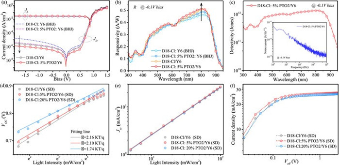
With respect to OSCs, the introduction of PTO2 via the sequential deposition method optimizes the vertical distribution of materials in the active layer, enhances the crystallinity of the polymer donor, which can increase the extraction efficiency of photogenerated carriers and improve the photovoltaic performance of the device. These optimizations, especially the improvement of donor crystallinity and packing at the interface between the active layer and hole transport layer, are of great importance for the construction of high-performance organic photodetectors (OPDs). To verify this deduction, OPDs with same active layer (or called as photosensitive layer) as above described have been developed, the detailed device performances are summarized in Table S4 (Supporting information). The current density measured under 1 sunlight irradiation and dark conditions are shown in Fig. 3a, as expected, the introduction of PTO2 in the D18-Cl domain via the sequential deposition method enhanced the crystallinity of the donors and reduced the opportunity of contact between Y6 and PEDOT:PSS, thus effectively suppressing the dark current of the OPD. Compared to the BHJ-based OPD, the photocurrent density (JL) of D18-Cl:PTO2/Y6 containing OPD is increased slightly, while the dark current density (JD) is reduced by more than 1 order of magnitude. Hence, the current on/off ratio of the optimized OPD reached 7 × 10⁵ at −0.1 V bias, which is much higher than that of the counterpart (9 × 10⁴). EQE and relevant responsivity (R) curves of the OPD operating at −0.1 V bias are shown in Fig. S4 (Supporting information) and Fig. 3b, respectively. From the EQE plots, it can be concluded that the introduction of PTO2 by the sequential deposition method can improve the photoresponse of OPDs, which in agreement with the above photovoltaic devices. Fig. S5 (Supporting information) depict the EQE curves of the optimized OPDs under different bias, as the reverse bias increases, the EQE values of the device show a slight increase. The R can be calculated from EQE as follows [39]:
Figure 3
Figure 3.
Electrical characterization of organic photodetectors. (a) J-V curves of OPDs in 1 sunlight irradiated and dark conditions. (b) Responsivity and (c) specific detectivity of D18-Cl:5%PTO2/Y6-based OPD, the insert is noise spectral density curve. (d) VOCversus light intensity curves, (e) JSCversus light intensity curves and (f) current density versus efficient voltage curves of binary and ternary devices based on sequential deposition method.
where EQE is above measured values, q is the electron charge, λ is the incident light wavelength, h is Plank's constant and c is the velocity of light. D18-Cl:PTO2/Y6 containing OPD achieved a maximum R of 0.52 A/W at 810 nm, which is higher than that of binary BHJ- based OPD (0.46 A/W). In addition to EQE and R, Detectivity (D*) is another key parameter to determine the detection performance of the OPD. In general, the comparatively accurate D* can be evaluated by the equation [40]:
(2)
where R is above calculated responsivity, A is the active device area and Sn is the noise current spectral density. We tested the noise current spectral density at the bias of −0.1 V as shown in the inserted graph of Fig. 3c. The noise current of the optimized OPD is 5.82 × 10⁻¹⁴ A Hz−1/2 at 70 Hz (corresponding to the frequency of the EQE measurement). Thus, the specific D* of the optimized OPD can be obtained as shown in Fig. 3c. At −0.1 V bias, the optimized OPD achieved a maximum D* of 1.34 × 10¹² Jones. The response speeds of the two types of OPDs is evaluated by measuring the rise times of the devices under a square-wave pulse of 808 nm laser. As shown in Figs. S6a and b (Supporting information), BHJ-based ternary OPD depicted a rise time of 70 µs, while in sequential deposition method performed OPD, the rise time was cut to 50 µs. The reduced rise time indicates that the introduction of PTO2 is conductive to enhance the response speed of OPDs.
To unravel the critical importance of introducing PTO2 on the charge dynamics process of optoelectronic devices, we investigated the influence of PTO2 on the charge transport characteristics of the devices by using the space-charge limited current (SCLC) method. Firstly, we investigated the hole transport properties of pure D18-Cl film and D18-Cl:PTO2 blended film, as shown in Fig. S7a (Supporting information). The pure D18-Cl-based hole-only device showed a hole mobility (μh) of 2.65 × 10⁻⁴ cm2 V−1 s−1, when 5%PTO2 was added to D18-Cl, the μh of the blend was elevated to 3.78 × 10⁻⁴ cm2 V−1 s−1, which could be attributed to the enhanced crystallinity and stacking property of the donors as can be supported by the morphological analysis below. The μh of the blend system decreased with the addition of excess PTO2 (20% content), which may be due to excessive phase separation leading to some interfacial contact problems. Furthermore, we measured the μh and electron mobility (μe) of D18-Cl/Y6- and D18-Cl:PTO2/Y6-based devices, as shown in Figs. S7b and c (Supporting information), corresponding mobility values are inserted in the relevant figures. D18-Cl:5%PTO2/Y6 contenting device showed a μh of 3.48 × 10⁻⁴ cm2 V−1 s−1, which is slightly lower than single donor (D18-Cl:5%PTO2) -based device. This is because the Y6 layer spin- coated by the sequential deposition method caused some hindrance to the hole transport. The μe of D18-Cl/Y6-, D18-Cl:5%PTO2/Y6- and D18-Cl:20%PTO2/Y6-based devices were calculated to be 2.48 × 10⁻⁴, 3.68 × 10⁻⁴ and 8.56 × 10⁻⁵ cm2 V−1 s−1, respectively. It can be clearly seen that 5%PTO2 optimized device exhibited balanced charge transport, which is responsible for high FF. The charge transport characteristics of BHJ-based devices are shown in Figs. S7d and e (Supporting information), PTO2-doped ternary film showed a μh of 3.31 × 10⁻⁴ and a μe of 3.73 × 10⁻⁴ cm2 V−1 s−1, respectively, which is slightly higher than that of binary BHJ-contained film (3.23 × 10⁻⁴ cm2 V−1 s−1 for μh and 3.06 × 10⁻⁴ cm2 V−1 s−1 for μe). The exciton-dissociation and charge recombination are investigated by measuring the relationship between VOC/JSC and light intensity (Plight). The VOC and Plight follow the relation [41]:
(3)
where kB is Boltzmann constant, T is Kelvin temperature and β is the recombination factor. As β gets closer to 1, the trap-assisted recombination gets smaller. As shown in Fig. 3d, With the increase of PTO2 content, β showed a decreasing trend, indicated that the introduction of PTO2 could suppress the trap-assisted recombination of the organic optoelectronic devices. Similar conclusions can be drawn in binary and ternary BHJ-based OSCs, as shown in Fig. S8a (Supporting information). The relationship between JSC and Plight is described as [42]:
(4)
Here α is related to bimolecular recombination. Fig. 3e and Fig. S8b (Supporting information) depict the JSCversusPlight curves of the binary and ternary devices fabricated by sequential deposition method and based on BHJ structure, respectively. All devices exhibited similar α value around 0.96, implied that bimolecular recombination is not dominant energy loss in these devices. The exciton dissociation and charge extraction of organic photoelectronic devices can be evaluated by analyzing the photocurrent density (Jph) versus effective voltage (Veff) characteristics (Fig. 3f and Fig. S8c in Supporting information). Jph is the margin between the photocurrent density measured under simulated sunlight and in the dark. Veff is the difference between V0 and Vapp, where V0 is the voltage when Jph is 0, Vapp is the applied voltage. Typically, the Jph with Veff larger than 2 V is considered to be the saturation current density (Jsat), the exciton dissociation ratio and charge collection ratio can be calculated by JSC/Jsat and Jpower/Jsat, where Jpower is obtained at maximum output power. The JSC, Jsat, Jpower and related ratios are listed in Table S5 (Supporting information). D18-Cl/Y6-, D18-Cl:5%PTO2/Y6- and D18-Cl:20%PTO2/Y6-based devices displayed close JSC/Jsat values, among them, 5%PTO2 added device obtained the maximum exciton dissociation efficiency of 96.5%. The results indicate that sequential deposition process optimizes the vertical distribution of the active layer component while still ensuring excellent donor/acceptor contact. Particularly, 5%PTO2 addition not only strengthens the original charge transport channel, but also provides additional donor/acceptor contacts to improve the exciton dissociation efficiency of the device, thus it is an effective way to enhance the device performance. For BHJ-based OSCs, binary and ternary devices showed high exciton dissociation efficiency of 96.4% and 97%, respectively, which is attributed to the homogeneous distribution of donor and acceptor in the BHJ. The charge collection efficiencies for D18-Cl/Y6, D18-Cl:5%PTO2/Y6 and D18-Cl:20%PTO2/Y6-based devices were calculated to be 87.7%, 89.3% and 85.1%, respectively. 5%PTO2 added device achieved the maximum charge collection efficiency that is attributed to the improved donor crystallinity. However, when the content of PTO2 increased to 20%, the charge collection efficiency decreased to 85.1%, which is due to the excessive introduction of PTO2 caused inferior interfacial contact. OSCs based on BHJ structure achieved a relatively low charge collection efficiency (82.5% for binary OSC and 83.8% for ternary OSC), which also indicates the importance of the crystallinity and stacking modulation of active layer materials for the charge extraction process.
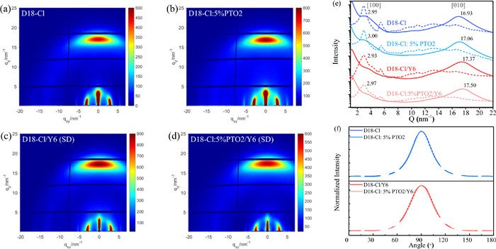
The essence of the enhancement of charge dynamics processes in organic optoelectronic devices depend on the optimization of the active layer/photosensitive layer in the aspect of material vertical distribution, crystallization, stacking and micro-morphology. For demonstrating the effect of the introduction of PTO2 on the micro-morphology of the co-blended films constructed with the dual donors, we first investigated the films using atomic force microscope (AFM) and transmission electron microscopy (TEM) as shown in Fig. S9 (Supporting information). The root-mean-square (RMS) surface roughness of D18-Cl-based film is 2.03 nm, when PTO2 was added in D18-Cl, the RMS values increased to 2.09 nm for D18-Cl:5%PTO2-based film and 2.19 nm for D18-Cl:20% PTO2-based film. The increased RMS values along with gradual sharpening of the light and dark fluctuation of AFM images is attributed to the enhanced crystallinity of donors. Similar to the AFM results, the TEM images also reflect a similar regularity. PTO2 optimized donor film showed more homogeneous material distribution and more distinct phase separation boundary (Figs. S9d–f). The influence of the introduction of PTO2 on the crystallinity of the donor phase was further investigated by using Grazing-incidence wide-angle X-ray scattering (GIWAXS). Figs. 4a–d depict the 2D GIWAXS patterns of D18-Cl, D18-Cl:5%PTO2, D18-Cl/Y6 and D18-Cl:5%PTO2/Y6-based films, relevant 1D linecut profiles and azimuthal integrated curves are exhibited in Figs. 4e and f. The characteristic peaks and the relevant parameters obtained from the calculations are shown in Tables S6 and S7 (Supporting information). Pure D18-Cl film revealed a distinct (010) peak at 16.93 nm−1 in the out-of-plane (OOP) direction, which corresponded to a π-π stacking distance of 3.71 Å. This favorable face-on orientation is beneficial to hole transport. In the in-plane (IP) direction, the signal appearing at 2.95 nm−1 corresponded to the arc acceptance. As 5%PTO2 was introduced into D18-Cl, the signal in the OOP direction was shifted to 17.06 nm−1, indicating the π-π stacking distance was reduced to 3.68 Å. Similarly, (100) peak also showed narrowed stacking distance. The results indicated that the introduction of PTO2 could enhance the stacking compactness of the donor. The crystallinity can be further estimated by calculating the crystalline coherence length (CCL) values with the Scherrer equation [43]. The calculated CCL values of (010) and (100) peaks are summarized in Tables S6 and S7. Compared to D18-Cl-based film, D18-Cl:5%PTO2 containing film exhibited an increased CCL value in both OOP (from 29.64 Å to 29.96 Å) and IP directions (from 132.15 Å to 140.47 Å). From the comparison of pure donor phases, we conclude that the introduction of PTO2 into D18-Cl not only reduces the stacking distance of the donors and thus improves the hole transport efficiency, but also enhances the crystallinity of the donors, which is conductive to decrease the dark current density of the optoelectronic devices. When the Y6 precursor solution was dripped on the surface of D18-Cl film, the (010) peak of the D8-Cl/Y6 hybrid film was shifted to 17.37 nm−1 which corresponded to the scattering signal of Y6 in the OOP direction. The calculated stacking distance and CCL values were 3.62 Å and 25.66 Å, respectively. As for the (100) peak, D8-Cl/Y6 exhibit similar peak but relatively different CCL values as revealed in Table S6, which is caused by the flushing of the Y6 solution on the donor layer. For D8-Cl:5%PTO2/Y6 films, the (010) signal was obtained at 17.50 nm−1, suggested a smaller π-π stacking distance of 3.59 Å compared to that of D18-Cl/Y6 film. The decreased π-π stacking distance may be due to the compact stacking of the D18-Cl:PTO2 layer that guided the ordered deposition of Y6. The (100) signal of D8-Cl:5%PTO2/Y6 film also showed similar peak but much smaller CCL values compared to D18-Cl:5%PTO2 film by the same reason. Furthermore, the influence of introducing PTO2 on face-on to edge-on ratios have been studied via analyzing the pole curves extracted from (010) and (100) scattering peaks. As shown in Fig. 4f and Fig. S10 (Supporting information), the azimuthal angle refers to the angle between the crystallographic orientation and the substrate, and the 90° corresponds to the qz-axis direction. It is evident that all films exhibited a perfect face-on orientation and the introduction of a moderate amount of PTO2 did not hinder the efficient charge transport in the active layer/photosensitive layer.
Figure 4
Figure 4.
Study on molecular crystallization and stacking properties. 2D GIWAXS patterns of (a) D18-Cl film, (b) D18-Cl:5%PTO2 film, (c) D18-Cl/Y6 film and (d) D18-Cl:5%PTO2 film. (e) 1D linecut profiles at OOP and IP direction of above films. (f) Corresponding pole curves extracted from (010) scattering peaks.
In summary, we demonstrate a novel and effective strategy for constructing high performance organic optoelectronic devices by using eutectic donors (D18-Cl:PTO2) as the first layer in sequential deposition process. The introduction of PTO2 endowed the donor phase with high crystallinity and compact packing, which can induce the orderly deposition of the acceptor Y6. The optimized distribution, crystallization and stacking properties of the constituent materials of active layer at the surface of PEDOT:PSS is conductive to enhance charge transport and extraction efficiencies of the device. Utilizing this strategy in OSCs, a high PCE of 17.65% with good light-degradation stability has been realized, which is superior to that of the binary or ternary OSC based on conventional BHJ structure. As for OPDs, this method can effectively reduce the dark current of the device by more than an order of magnitude and enhance the responsivity to 0.52 A/W. Additionally, the active layer constructed by this method does not require additional post-treatment, which reduces the manufacturing cost and process complexity of organic optoelectronic devices, exhibiting great potential for commercial production.
Declaration of competing interest
The authors declare that they have no conflict of interest.
Acknowledgments
The work was supported by the National Natural Science Foundation of China (NSFC, Nos. 62075029, 52130304, 62105055 and U2032128), the International Cooperation and Exchange Project of Science and Technology Department of Sichuan Province (No. 2020YFH0063). The China Postdoctoral Science Foundation (Nos. 2020TQ0058 and 2021M7006). the Fundamental Research Funds for the Central Universities (No. ZYGX2021J017). Shanghai Natural Science Foundation (No. 19ZR1463300).
Supplementary materials
Supplementary material associated with this article can be found, in the online version, at doi:10.1016/j.cclet.2022.06.064.
[1]
C. Fuentes-Hernandez, W.F. Chou, T.M. Khan, et al., Science 370 (2020) 698-701. doi: 10.1126/science.aba2624
[2]
R. Su, S.H. Park, X. Ouyang, et al., Sci. Adv. 8 (2022) eabl8798. doi: 10.1126/sciadv.abl8798
[3]
Y. Park, C. Fuentes-Hernandez, K. Kim, et al., Sci. Adv. 7 (2021) eabj6565. doi: 10.1126/sciadv.abj6565
Figure 1
(a) Molecular structures of D18-Cl, PTO2 and Y6. (b) Schematic illustration of sequential deposition process. (c) Energy level diagrams of D18-Cl, PTO2 and Y6. (d) Absorption spectra of D18-Cl, PTO2, Y6, D18-Cl/Y6 and D18-Cl:PTO2/Y6 films. (e) PL spectra of D18-Cl, PTO2 and D18-Cl:PTO2 (1:1) films.
Figure 2
Electrical characterization of organic solar cells. (a) J-V curves of binary and ternary OSCs based on BHJ structure. (b) J-V curves of control and optimized OSCs based on sequential deposition process. (c) Histogram of the PCEs of D18-Cl:Y6 (BHJ), D18-Cl:PTO2:Y6 (BHJ), D18-Cl/Y6 (SD) and D18-Cl:PTO2/Y6 (SD)-based OSCs, fitted with Gaussian distributions (solid lines). (d) EQE curves of binary and ternary OSCs based on BHJ structure. (e) EQE curves of control and optimized OSCs based on sequential deposition process. (f) Device stability under 100 mW/cm2 for 150 min.
Figure 3
Electrical characterization of organic photodetectors. (a) J-V curves of OPDs in 1 sunlight irradiated and dark conditions. (b) Responsivity and (c) specific detectivity of D18-Cl:5%PTO2/Y6-based OPD, the insert is noise spectral density curve. (d) VOCversus light intensity curves, (e) JSCversus light intensity curves and (f) current density versus efficient voltage curves of binary and ternary devices based on sequential deposition method.
Figure 4
Study on molecular crystallization and stacking properties. 2D GIWAXS patterns of (a) D18-Cl film, (b) D18-Cl:5%PTO2 film, (c) D18-Cl/Y6 film and (d) D18-Cl:5%PTO2 film. (e) 1D linecut profiles at OOP and IP direction of above films. (f) Corresponding pole curves extracted from (010) scattering peaks.

 DownLoad:

 下载:
下载:


