Citation:
Zhan-Bing YANG, Su-Bing YANG, Xiao-Jian QU, Tamaki SHIBAYAMA, Seiichi WATANABE. Development of Laser-HVEM and Its Application on In-situ Observation on Lattice Defects Behavior[J]. Chinese Journal of Structural Chemistry,
2020, 39(4): 623-629.
doi:
10.14102/j.cnki.0254-5861.2011-2824
Development of Laser-HVEM and Its Application on In-situ Observation on Lattice Defects Behavior
Received Date:
15 March 2020 Accepted Date:
03 April 2020 Available Online:
01 April 2020
Fund Project:
Abstract:
A nanosecond pulse laser source head (Nd: YAG laser, Inlite Ⅱ-20, Continuum) was equipped to a high-voltage electron microscope (HVEM, Hitachi, H-1300) to develop a laser-HVEM system at Hokkaido University. Using the laser-HVEM, new methods for in-situ observation on the formation process of laser-induced lattice point defects at the internal of crystalline solid are achieved; some striking phenomena and potential mechanisms are explored. In the present paper, we review our progresses on in-situ experiments of lattice defects behavior in metal using the laser-HVEM. These progresses are expected to provide insight for a broader application of laser-HVEM in scientific research.
The high-voltage electron microscope (HVEM) has been a powerful instrument for radiation damage studies since its development in the 1960s due to its ability to simulate neutron irradiation by introducing Frenkel pairs (FPs, referring to an interstitial atom and vacancy) under electron beam irradiation[1-3]. By simulation, the interaction of lattice point defects, i.e. interstitial atom and vacancy, can be well understood, which is essential and greatly useful for exploring the interaction mechanisms that govern the changes of both microstructure[4-6] and mechanical properties[7] of the materials under a radiation environment.
The most important advantage of HVEM in radiation damage studies is in-situ observation which directly and continuously records the evolution process of the non-equilibrium phenomena during irradiation and is thus beneficial for determining the driving mechanism[8]. Moreover, due to its large chamber, HVEM allows for convenient connection and interfacing with other instruments, such as an accelerator, which eliminates the main limitation of HVEM, that is, the collision cascades cannot be introduced; furthermore, the large chamber of HVEM allows for in-situ observation during multi-beam irradiation[9-12]. In the real irradiation environment, FPs and an additional source of vacancies coexist (e.g., neutron, heavy ion, γ-ray, and electron). However, for a vacancydominated study, the effect of solo vacancy behaviour has not yet been observed in-situ.
Vacancy can be introduced in a crystalline solid by quenching[13]. Materials are rapidly heated by a pulsed laser beam irradiation and then cooled during the interval of two successive pulses, which results in rapid self-quenching and re-solidification[14]. In addition, the small bulk of a laser head allows it to be conveniently connected with HVEM. Therefore, a HVEM equipped with a laser head system (laser-HVEM) was developed at Hokkaido University in 2007[15], which allowed for in-situ observation during electron-photon (controllable high-energy laser beam) dual-beam irradiation.
In the present paper, we review some results of our studies[15-19], which employed the laser-HVEM system, including the lattice point defects behaviors in face centered cubic (F.C.C.) metal. In the future, laser-HVEM is expected to be employed for a broader research.
2.
INTRODUCTION OF THE NEW DEVELOPED LASER-HVEM SYSTEM
A Nd: YAG pulse laser (Inlite Ⅱ-20, Continuum) is used in the present laser-HVEM; intensity of the incidence laser beam is controlled by selecting various central wavelengths (λ) of the beam, such as 266, 355, 532, 1064 nm, etc.; the highest pulse repetition rate is 20 Hz; duration of each pulse is 5~6 ns. The employed HVEM is H-1300 (Hitachi); acceleration voltage is 1300 kV; the point-to-point resolution is 0.204 nm; and the degree of vacuum during irradiation is 1.2 × 10⁻⁵ Pa[15].
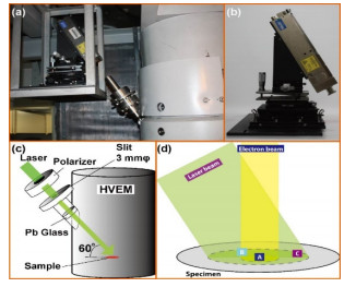
Real photograph and schematic of the system are shown in Fig. 1a and 1c, respectively. The laser source head (Fig. 1b) is installed to the HVEM chamber with an angle of 30° above the sample position; accordingly, the linearly polarized laser beam passes through a quartz window and irradiates the transmission electron microscope (TEM) sample with an angle of 60°. Laser beam position is controlled by adjusting the bracket in the direction of x and z, as well as rotating and tilting. The diameter of laser beam in this study was measured to be 1.5~2 mm; the typical diameter of electron beam for irradiation is approximately 2 μm.
Figure 1
Figure 1.
Laser-HVEM system. (a) Photograph of the system. (b) Laser source head on the bracket. (c) Schematic of the system[16]. Copyright of NPG. (d) Schematic of the laser-electron simultaneous dual-beam irradiation of aTEM specimen[20]. Copyright of Elsevier Area A: centre of the dual-beam irradiation, where the intensity of the electron beam is the highest. Area B: edge of the dual-beam irradiation area where the electron beam intensity is weaker than that of area A but the intensity of the laser beam is maintained. Area C: electron irradiation can be neglected here because of its significantly lower intensity, so this area can therefore be treated as a single laser beam irradiation area
Electron beam irradiation, laser-electron sequential irradiation (L→e- irr.), and laser-electron dual-beam irradiation are accomplished by using the Laser-HVEM. Because the diameter of the laser beam is larger than that of the electron beam, during dual-beam irradiation, the irradiation area is divided into three parts designated as A, B and C in Fig. 1d[20].
3.
STUDIES EMPLOYING THE LASER-HVEM
3.1
In-situ observation of dislocation loop evolution during laser and/or electron beam irradiation
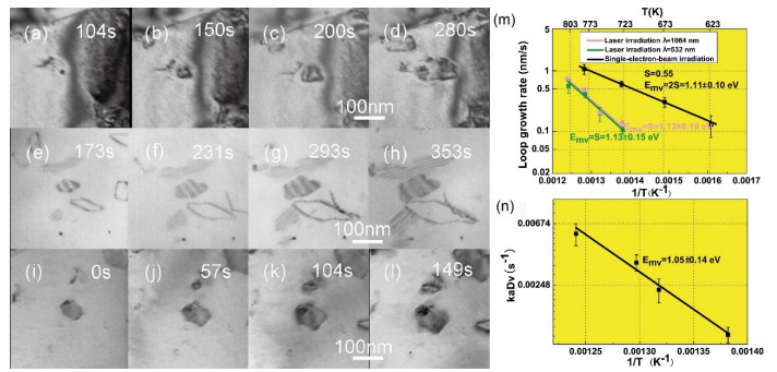
Formation of interstitial type (Ⅰ-type) dislocation loop is usually observed in-situ during electron beam irradiation using HVEM, as shown in Fig. 2a to 2d. Methods generally used for introducing vacancy, such as high-energy-particle irradiation, plastic deformation or thermal quenching[13, 21, 22], are unsuitable for in-situ observation, since the clustering of vacancies into dislocation loops may occur rapidly when point defects become excessive. Using laser-HVEM, the first in-situ observation of vacancy type (Ⅴ-type) dislocation loop formation was reported by us in the reference during laser irradiation and the sequential annealing on an F.C.C. crystal (i.e. SUS316L steel)[16]. Mechanism of Ⅴ-type loop formation under laser irradiation was explained, in which the pulsed laser irradiation mainly introduceed excessive vacancies at the surface of the sample due to the quick heating and quenching effect; and the excessive vacancies consequently diffused into the internal of the sample to form the Ⅴ-type loops, as shown in Fig. 2e to 2h. The loops formed during the previous laser beam irradiation (Fig. 2i) continuously grew during the sequential thermal annealing (Fig. 2j to 2l), because the existing excessive vacancies at the surface can still thermally migrate to the interior of the sample and contribute to the loops growth.
Figure 2
Figure 2.In-situ observation of dislocation loops growth in SUS316L steel during various irradiations using laser-HVEM, and experiment results of the two new methods for measuring Emv[16]. Copyright of NPG (a)~(d) Ⅰ-type loop growth during electron single irradiation at 726 K, which is a typical method for in-situ observation of Ⅰ-type loop formation in F.C.C. metal; (e)~(h) Ⅴ-type loop growth during laser irradiation at 806 K (λ = 532 nm); (i)~(l) Ⅴ-type loop growth during the sequential thermal annealing at 780 K after laser irradiation at the same temperature (λ = 1064 nm). (m) The first new method, temperature dependence of the Ⅴ-type loop growth rate under laser single beam irradiation with different λ (532 nm, 2 Hz, energy density = 0.24 kJ/m2, and 1064 nm, 2 Hz, energy density = 1.04 kJ/m2). Dark line is induced from electron irradiation according to Kiritani[1]; (n) The second new method, Arrhenius plots of the exponential factor in equation based on the temperature dependence of Ⅴ-type loop growth rate during thermal annealing
In the 1970s, Kiritani et al.[1] proposed a method of measuring the activation energy for vacancy migration (Emv) from the temperature dependence of the Ⅰ-type loop growth rate in an in-situ experiment involving electron beam irradiation using an HVEM, which is presently the generally used method for the measure of Emv.
As shown in Fig. 2e to 2h and 2I to 2l, the in-situ observation on Ⅴ-type dislocation loop is accomplished during laser irradiation and sequential annealing using laser-HVEM; subsequently, two new methods on measuring Emv were proposed by the temperature dependence of the Ⅴ-type loop growth rate[16], which breaks new ground after little advance for 30 years in this field. The first new method is directly induced by the temperature dependence of the Ⅴ-type loop growth rate under continuous pulsed-laser beam irradiation, as equation (1) shows:
where R is the loop radius, Dv is the vacancy diffusivity, $ k $ is the Boltzmann constant, and T is the working temperature.
The second new method is driven from the sequential thermal annealing. Excess vacancies are no longer generated during thermal annealing after irradiation by successive laser pulses, and the number of excess vacancies gradually decreased due to annihilation of vacancies at internal sinks. The change in loop size due to thermal annealing can be expressed as:
where R0 is the loop radius at the measurement start time during thermal annealing, CV, excess is the initial concentration of vacancies causing Ⅴ-type loops to grow in the interior of the sample prior to thermal annealing, b is the magnitude of the Burgers vector, and kα is the sink strength with the contribution of all other microstructures with the foil sample. The Arrhenius slops in Fig. 2m and 2n are the experimental results of Emv obtained from laser irradiation and thermal annealing, respectively. And the results are in good agreement with previous reports[23, 24].
3.2
Void formation under various irradiations and effective swelling control under dual-beam irradiation
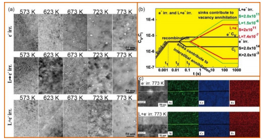
Void swelling causes changes in dimensio and remains a major limitation for the performance cladding materials[25, 26]. For void nucleation, it is necessary to reach a definite critical vacancy concentration depending on temperature[27] and void formation is governed by point defects introduced through irradiation[28]. Using Laser-HVEM, void formation under laser and/or electron beam was studied for controlling or depressing void swelling. The results obtained from electron beam irradiation are treated as a standard due to the thorough investigation of void swelling behavior under electron-beam irradiation[17, 18]. Excess vacancies introduced by single laser beam irradiation enhance void nucleation but contribute less to void growth[17]. In Fig. 3, for L → e- irr., due to the enhanced nucleation, the number of voids is more than that under e- irr. The voids nucleated under pre-pulsed laser irradiation may preferentially grow up during the sequential e- irr. Subsequently, void swelling, representing the comprehensive results for void mean size and number density, increases significantly. However, compared with single electron irradiation, laser and electron dual-beam irradiation showed a striking effect of 1 + 1 < 1 on the void swelling, see Fig. 3a. Calculation on time dependences of concentration of vacancy (CV) and interstitial (CI) under electron irradiation and dual-beam irradiation shows that the recombination of excess vacancy and interstitial atom is greatly enhanced by the simultaneous irradiation, and acts as the dominant governing mechanism of the defect behaviour, as shown in Fig. 3b[17].
Figure 3
Figure 3.
(a) Void micrographs in SUS316L steel under different irradiation conditions[18]. Copyright of Elsevier (λ = 532 nm, 2 Hz, energy density = 0.24 kJ/m2). (b) Calculated time dependences of CV and CI under electron irradiation and laser-electron dual-beam irradiation for 20 min[17]. Copyright of NPG. (c) Mapping results of components near random grain boundary under electron irradiation and dual-beam irradiation at 773 K
Additionally, element diffusion is governed by interstitial and vacancy, and radiation induced segregation (RIS) is inevitable in the cladding materials. In SUS316L steel, due to the I + V = 0, segregation of Cr and Ni near the random grain boundary under dual-beam irradiation is lower than that under electron irradiation. The ratio of vacancy flux of dual-beam irradiation to that of electron irradiation is 45.7%[29].Therefore, the dual-beam irradiation proposes a method on depressing void swelling and RIS substantially in crystalline solids.
3.3
Effect of laser irradiation on the crystal surface
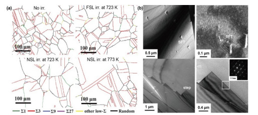
Femtosecond laser (FSL) and nanosecond laser (NSL) irradiation was carried out on SUS316L austenitic stainless steel to explore the effect of laser irradiation on surface modification suing laser-HVEM at suitable temperature[19]. Analysis result of electron backscatter diffraction (EBSD) is shown in Fig. 4a. Compared with non-irradiated specimens, laser irradiations enhanced the proportion of coincident site lattice (CSL) boundaries, especially twins, which would subsequently enhance the inter-granular corrosion resistance[30]. In Fig. 4b, the "stepped" boundaries with head-to-tail connections were analyzed to be twin boundaries, and the stacking fault tetrahedra (SFTs, vacancy-type lattice defect) are observed on the "stepped" boundaries instead of inside the twin. The change of CSL boundary ratio is mainly related to grain boundary migration and twins' formation. Energy generated by the pulsed laser irradiation provides favourable conditions for the grain boundary migration in the skin layer of specimens, and the crystal defects caused during irradiation promote the nucleation and growth of twins during grain boundary migration[31].
Figure 4
Figure 4.
(a) Electron backscatter diffraction analysis on grain boundary characteristic distribution after laser irradiations[19]. Copyright of Surface Technology. Compared with non-irradiated specimens, the pro portion of twins after femtosecond and nanosecond laser irradiation at 723 K increased by 2.88% and 10.78%, respecttively; random grain boundary decreased by 4.24% and 9.97%, respectively. After nanosecond laser irradiation at 773 K, the proportion of twins increased by 12.52% and random grain boundary decreased by10.68%. (b) TEM image of SFT and twin boundary after nanosecond laser irradiation sample at 773 K[19]: Copyright of Surface Technology. Z-contrast diagram of high angle annular dark field of SFT shows a pyramidal shape; continuous "steps" formed at grain boundaries and were analyzed to be twin boundary by selectedarea electron diffraction
Laser-HVEM provided new research methods for materials science, which is beneficial to well understand some unknown mechanisms. To date, using laser-HVEM, in-situ observation of interaction between excess vacancies and Frenkel pairs and defect structure changes governed by lattice point defects in a crystal is possible[16]. In addition, in-situ observation of self-organization structures on semiconductors' surface is achieved and, new mechanism which can well explain formation of LIPSS was proposed[15, 32, 33, 34].
As to the prospects in instrument development, laser-HVEM is firstly expected to be connected with accelerators for in-situ observation of photonelectron-ion multi-beam irradiation for further irradiation damage study; in the aspects of application, laser-HVEM is anticipated to be employed in the studies of defect behaviour in crystalline solids, surface modification of semiconductors, and in a broader scientific research, such as nanotechnology, space science and irradiation effect on polymer materials and foods.
ACKNOWLEDGEMENT:
The authors are grateful to Professors M. Kawai, N. Sakaguchi, H. Takahashi, and Dr. T. Kato for helpful discussions regarding the presented results.
[1]
Kiritani, M.; Yoshida, N.; Takata, H.; Maehara, Y. Growth of interstitial type dislocation loops and vacancy mobility in electron-irradiated metals. J. Phys. Soc. Jpn. 1975, 38, 1677–1686. doi: 10.1143/JPSJ.38.1677
[2]
Makin, M.; Sharp, J. An introduction to high-voltage electron microscopy. J. Mater Sci.1968, 3 360–371. doi: 10.1007/BF00550979
[3]
Foreman, A.; Makin, M. Effect of vacancy loops on swelling of irradiated materials. J. Nucl. Mater.1979, 79, 43–57. doi: 10.1016/0022-3115(79)90432-X
[4]
Zinkle, S.; Was, G. Materials challenges in nuclear energy. Acta Mater. 2013, 61, 735–758. doi: 10.1016/j.actamat.2012.11.004
[5]
Sakaguchi, N.; Watanabe, S.; Takahashi, H. Heterogeneous dislocation formation and solute redistribution near grain boundaries in austenitic stainless steel under electron irradiation. Acta Mater.2001, 49, 1129–1137. doi: 10.1016/S1359-6454(01)00031-3
[6]
Zhang, Z.; Liu, C.; Wang, X.; Miller, M.; Ma, D.; Chen, G.; Williams, J.; Chin, B. Effects of proton irradiation on nanocluster precipitation in ferritic steel containing fcc alloying additions. Acta Mater.2012, 60, 3034–3046. doi: 10.1016/j.actamat.2012.02.008
[7]
Nishiyama, Y.; Onizawa, K.; Suzuki, M.; Anderegg, J.; Nagai, Y.; Toyama, T.; Hasegawa, M.; Kameda, J. Effects of neutron-irradiation-induced intergranular phosphorus segregation and hardening on embrittlement in reactor pressure vessel steels. Acta Mater.2008, 56, 4510–4521. doi: 10.1016/j.actamat.2008.05.026
[8]
Kiritani, M.; Takata, H. Dynamic studies of defect mobility using high-voltage electron-microscopy. J. Nucl. Mater.1978, 69–70, 277–309.
[9]
Taylor, A.; Wallace, J.; Ryan, E.; Philippides, A.; Wrobel, J. In-situ implantation system in argonne-national-laboratory hvem-tandem facility. Nucl. Instrum. Methods Phys. Res.1981, 189, 211–217. doi: 10.1016/0029-554X(81)90148-8
[10]
Takeyama, T.; Ohnuki, S.; Takahashi, H. Study of cavity formation in 316-stainless steels by means of hvem ion-accelerator dual irradiation. J. Nucl. Mater.1985, 133, 571–574.
[11]
Furuya, K.; Mitsuishi, K.; Song, M.; Saito, T. In-situ, analytical, high-voltage and high-resolution transmission electron microscopy of Xe ion implantation into Al. J. Electron Microsc.1999, 48, 511–518. doi: 10.1093/oxfordjournals.jmicro.a023709
[12]
Delarubia, T.; Guinan, M. Progress in the development of a molecular-dynamics code for high-energy cascade studies. J. Nucl. Mater.1990, 174, 151–157. doi: 10.1016/0022-3115(90)90229-G
[13]
Kino, T.; Koehler, J. Vacancies and divacancies in quenched gold. Phys. Rev.1967, 162, 632–648. doi: 10.1103/PhysRev.162.632
[14]
Majumdar, J.; Galun, R.; Mordike, B.; Manna, I. Effect of laser surface melting on corrosion and wear resistance of a commercial magnesium alloy. Mater. Sci. Eng. A2003, 361, 119–129. doi: 10.1016/S0921-5093(03)00519-7
[15]
Watanabe, S.; Yoshida, Y.; Kayashi, S.; Yatsu, S. In-situ observation of self-organizing nanodot formation under nanosecond-pulsed laser irradiation on Si surface. J. Appl. Phys.2010, 108, 103510. doi: 10.1063/1.3512888
[16]
Yang, Z.; Sakaguchi, N.; Watanabe, S.; Kawai, M. Dislocation loop formation and growth under in-situ laser and/or electron irradiation. Sci. Rep. UK.2011, 1, 190. doi: 10.1038/srep00190
[17]
Yang, Z.; Watanabe, S.; Kato, T. The irradiation effect of a simultaneous laser and electron dual-beam on void formation. Sci. Rep. UK.2013, 3, 1201. doi: 10.1038/srep01201
[18]
Yang, S.; Yang, Z.; Wang, H.; Watanabe, S.; Shibayama, T. Effect of laser and/or electron irradiation on void swelling in SUS316L austenitic stainless steel. J. Nucl. Mater.2017, 488, 215–221. doi: 10.1016/j.jnucmat.2017.03.002
[19]
Qu, X.; Yang, Z.; Yang, S. Effect of pulsed laser irradiation on the coincidence site lattice grain boundary of 316L stainless steel. Surf. Technol.2019, 48, 201–208.
[20]
Yang, Z.; Watanabe, S. Dislocation loop foramtion under various irradiations of laser and/or electron beams. Acta Mater.2013, 61, 2966–2972. doi: 10.1016/j.actamat.2013.01.056
[21]
Davis, T.; Hirth, J. Nucleation rate of vacancy clusters in crystals. J. Appl. Phys.1966, 37, 2112–2116. doi: 10.1063/1.1708745
[22]
Davis, T. Nucleation rate of vacancy clusters in aluminum. J. Appl. Phys.1967, 38, 3756–3760. doi: 10.1063/1.1710206
[23]
Hidaka, Y.; Ohnuki, S.; Takahashi, H.; Watanabe, S. Effect of He on void formation and radiation-induced segregation in dual-beam irradiated Fe-Cr-Ni. J. Nucl. Mater.1994, 212, 330–335.
[24]
Pokor, C.; Brechet, Y.; Dubuisson, P.; Massoud, J. Irradiation damage in 304 and 316 stainless steels: experimental investigation and modeling. Part Ⅰ: evolution of the microstructure. J. Nucl. Mater.2004, 326, 19–29. doi: 10.1016/j.jnucmat.2003.11.007
[25]
Yvon, P.; Carré, F. Structural materials challenges for advanced reactor systems. J. Nucl. Mater.2009, 385, 217–222. doi: 10.1016/j.jnucmat.2008.11.026
[26]
Azevedo, C. Selection of fuel cladding material for nuclear fission reactors. Eng. Fall. Anal.2011, 18, 1943–1962. doi: 10.1016/j.engfailanal.2011.06.010
[27]
Yoshiie, T.; Cao, X.; Sato, K.; Miyawaki, K.; Xu, Q. Point defect processes during incubation period of void growth in austenitic stainless steels, Ti-modified 316SS, J. Nucl. Mater.2011, 417, 968–971. doi: 10.1016/j.jnucmat.2010.12.189
[28]
Sekio, Y.; Yamashita, S.; Sakaguchi, N.; Takahashi, H. Effect of additional minor elements on accumulation behavior of point defects under electron irradiation in austenitic stainless steels. Mater. Trans.2014, 55, 438–442. doi: 10.2320/matertrans.MD201309
[29]
Yang, S.; Yang, Z.; Wang, H. Effect of pulsed-laser and/or electron irradiation on vacancy diffusion in SUS316L austenitic stainless steel. Chin. J. Eng.2017, 39, 903–908.
[30]
Michiuchi, M.; Kokawa, H.; Wang, Z.; Sato, Y.; Sakai, K. Twin-induced grain boundary engineering for 316 austenitic stainless steel. Acta Mater.2006, 54, 5179–5184. doi: 10.1016/j.actamat.2006.06.030
[31]
Mahajan, S.; Pande, C.; Imam, A.; Rath, B. Formation of annealing twins in fcc crystals. Acta Mater.1997, 45, 2633–2638. doi: 10.1016/S1359-6454(96)00336-9
[32]
Yoshida, Y.; Watanabe, S.; Nishijima, Y.; Ueno, K.; Misawa, H.; Kato, K. Fabrication of a Au/Si nanocomposite structure by nanosecond pulsed laser irradiation. Nanotechnology2011, 22, 375607. doi: 10.1088/0957-4484/22/37/375607
[33]
Yoshida, Y.; Yatsu, S.; Watanabe, S.; Yamauchi, A.; Shibano, J. Transformation in iron-platinum thin film via nanosecond pulsed laser irradiation. J. Phys. Chem. Sol.2017, 109, 46-49. doi: 10.1016/j.jpcs.2017.05.013
[34]
Lei, Y. H.; Yu, R. X.; Shibayama, T.; Ishioka, J.; Watanabe, S. In-situ observation of self-assembly of quasi-two-dimensional Au nano-submicron particles on β-SiC substrates via nanosecond-pulsed laser irradiation-induced dewetting of thin Au films. Mater. Lett.2016, 164, 202–205. doi: 10.1016/j.matlet.2015.11.004
Figure 1
Laser-HVEM system. (a) Photograph of the system. (b) Laser source head on the bracket. (c) Schematic of the system[16]. Copyright of NPG. (d) Schematic of the laser-electron simultaneous dual-beam irradiation of aTEM specimen[20]. Copyright of Elsevier Area A: centre of the dual-beam irradiation, where the intensity of the electron beam is the highest. Area B: edge of the dual-beam irradiation area where the electron beam intensity is weaker than that of area A but the intensity of the laser beam is maintained. Area C: electron irradiation can be neglected here because of its significantly lower intensity, so this area can therefore be treated as a single laser beam irradiation area
Figure 2In-situ observation of dislocation loops growth in SUS316L steel during various irradiations using laser-HVEM, and experiment results of the two new methods for measuring Emv[16]. Copyright of NPG (a)~(d) Ⅰ-type loop growth during electron single irradiation at 726 K, which is a typical method for in-situ observation of Ⅰ-type loop formation in F.C.C. metal; (e)~(h) Ⅴ-type loop growth during laser irradiation at 806 K (λ = 532 nm); (i)~(l) Ⅴ-type loop growth during the sequential thermal annealing at 780 K after laser irradiation at the same temperature (λ = 1064 nm). (m) The first new method, temperature dependence of the Ⅴ-type loop growth rate under laser single beam irradiation with different λ (532 nm, 2 Hz, energy density = 0.24 kJ/m2, and 1064 nm, 2 Hz, energy density = 1.04 kJ/m2). Dark line is induced from electron irradiation according to Kiritani[1]; (n) The second new method, Arrhenius plots of the exponential factor in equation based on the temperature dependence of Ⅴ-type loop growth rate during thermal annealing
Figure 3
(a) Void micrographs in SUS316L steel under different irradiation conditions[18]. Copyright of Elsevier (λ = 532 nm, 2 Hz, energy density = 0.24 kJ/m2). (b) Calculated time dependences of CV and CI under electron irradiation and laser-electron dual-beam irradiation for 20 min[17]. Copyright of NPG. (c) Mapping results of components near random grain boundary under electron irradiation and dual-beam irradiation at 773 K
Figure 4
(a) Electron backscatter diffraction analysis on grain boundary characteristic distribution after laser irradiations[19]. Copyright of Surface Technology. Compared with non-irradiated specimens, the pro portion of twins after femtosecond and nanosecond laser irradiation at 723 K increased by 2.88% and 10.78%, respecttively; random grain boundary decreased by 4.24% and 9.97%, respectively. After nanosecond laser irradiation at 773 K, the proportion of twins increased by 12.52% and random grain boundary decreased by10.68%. (b) TEM image of SFT and twin boundary after nanosecond laser irradiation sample at 773 K[19]: Copyright of Surface Technology. Z-contrast diagram of high angle annular dark field of SFT shows a pyramidal shape; continuous "steps" formed at grain boundaries and were analyzed to be twin boundary by selectedarea electron diffraction

 DownLoad:

 下载:
下载:


